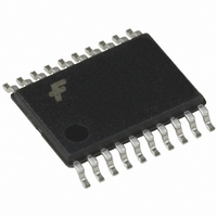
FMS6403MTC20X Fairchild Semiconductor, FMS6403MTC20X Datasheet

FMS6403MTC20X
Specifications of FMS6403MTC20X
FMS6403MTC20X_NL
FMS6403MTC20X_NLTR
FMS6403MTC20X_NLTR
Available stocks
Related parts for FMS6403MTC20X
FMS6403MTC20X Summary of contents
Page 1
... FSM6403MTC 0 to 70°C FSM6403MTC20X 0 to 70°C All packages are lead free per JEDEC: J-STD-020B standard. © 2005 Fairchild Semiconductor Corporation FMS6403 • Rev. 1.0.4 Description The FMS6403 offers comprehensive filtering for TV, set-top box, or DVD applications. This part consists of a triple, sixth-order filter with selectable 30MHz, 15MHz, or 8MHz cutoff frequency ...
Page 2
... Functional Block Diagram Typical Application © 2005 Fairchild Semiconductor Corporation FMS6403 • Rev. 1.0.4 Figure 1. Block Diagram Figure 2. Typical Application Circuit 2 www.fairchildsemi.com ...
Page 3
... Input Input CC © 2005 Fairchild Semiconductor Corporation FMS6403 • Rev. 1.0.4 Figure 3. Pin Configuration Description Selects the external SYNC_IN signal when set to logic 1; do not float. Selects RGB clamp levels when set to logic 1. YPbPr clamps levels when set to logic 0; do not float. ...
Page 4
... Fairchild does not recommend exceeding them or designing to Absolute Maximum Ratings. Symbol T Operating Temperature Range Range Input Source Resistance SOURCE © 2005 Fairchild Semiconductor Corporation FMS6403 • Rev. 1.0.4 Parameter Parameter Parameter 4 Min. Max. Unit -0.3 +6.6 -0 0.3 ...
Page 5
... INMUX Isolation MUXISO SNR Signal-to-Noise Ratio t Propagation Delay for SD pdSD T1 SYNC to SYNC_IN Delay SYNC_IN Minimum Pulse T2 Width Note: 3. 100% tested at 25°C. © 2005 Fairchild Semiconductor Corporation FMS6403 • Rev. 1.0.4 Conditions load RGB_SEL, 0dB_SEL, SELO SEL1 EXT_SYNC, IN2_SEL, SYNC_IN RGB_SEL, 0dB_SEL, ...
Page 6
... Gain, 0dB_SEL=1 f -1dB Bandwidth 1dBWB f -3dB Bandwidth CWB t Propagation Delay pdWB Note: 6. 100% tested at 25°C. © 2005 Fairchild Semiconductor Corporation FMS6403 • Rev. 1.0.4 =1, F =0, 0dB_SEL=0 (gain=6dB), R SEL0 SEL1 Conditions (4) All Channels PS Mode (4) All Channels PS Mode (4) All Channels All Channels ...
Page 7
... 0.1μF; all outputs AC coupled with 220μF into 150Ω, referenced to 400kHz; unless otherwise noted. Figure 4. SD Frequency Response Figure 6. SD Noise vs. Frequency © 2005 Fairchild Semiconductor Corporation FMS6403 • Rev. 1.0.4 =0, F =0, 0dB_SEL=0 (gain=6dB), R SEL0 SEL1 Figure 5. SD Group Delay vs. Frequency Figure 8 ...
Page 8
... 0.1μF; all outputs AC coupled with 220μF into 150Ω, referenced to 400kHz: unless otherwise noted. Figure 13. Bypass Mode Frequency Response © 2005 Fairchild Semiconductor Corporation FMS6403 • Rev. 1.0.4 =1, F =0, 0dB_SEL=0 (gain=6dB), R SEL0 SEL1 Figure 10. PS Group Delay vs. Frequency ...
Page 9
... SYNC_IN pin. If there is no video signal present, therefore no sync signal present, there must be an input © 2005 Fairchild Semiconductor Corporation FMS6403 • Rev. 1.0.4 applied to the SYNC_IN pin. When there is no video signal on the video inputs, SYNC_IN can be a sync pulse every 60μ ...
Page 10
... Tri-level sync may only be compressed 5 sync is compressed more than 5%, it may not be properly located. © 2005 Fairchild Semiconductor Corporation FMS6403 • Rev. 1.0.4 Sync Timing Normally, the FMS6403 responds to bi-level sync and clamps the sync tip during period ‘B’ in Figure 19. When ...
Page 11
... Video level does not include damp voltage, which offsets the input above ground. Table 4. Sync Settings EXT_SYNC, Pin Table 5. Clamp Settings RGB_SEL, Pin © 2005 Fairchild Semiconductor Corporation FMS6403 • Rev. 1.0.4 Sample Period (T) A Rate 13.5MHz 74ns 20T=1.5µs 27 MHz ...
Page 12
... The output drive configuration must be considered when calculating overall power dissipation. Care must be taken not to exceed the maximum die junction temperature. The following example can be used to © 2005 Fairchild Semiconductor Corporation FMS6403 • Rev. 1.0.4 calculate the FMS6403’s power dissipation and internal temperature rise: ...
Page 13
... Package drawings are provided as a service to customers considering Fairchild components. Drawings may change in any manner without notice. Please note the revision and/or date on the drawing and contact a Fairchild Semiconductor representative to verify or obtain the most recent revision. Package specifications do not expand the terms of Fairchild’s worldwide terms and conditions, specifically the warranty therein, which covers Fairchild products. Always visit Fairchild Semiconductor’ ...
Page 14
... Fairchild Semiconductor Corporation FMS6403 • Rev. 1.0.4 14 www.fairchildsemi.com ...


