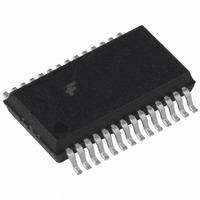
FMS6501MSA28X Fairchild Semiconductor, FMS6501MSA28X Datasheet

FMS6501MSA28X
Specifications of FMS6501MSA28X
FMS6501MSA28X_NL
FMS6501MSA28X_NLTR
FMS6501MSA28X_NLTR
Available stocks
Related parts for FMS6501MSA28X
FMS6501MSA28X Summary of contents
Page 1
... Automotive (In-Cabin Entertainment) Ordering Information Part Number Pb-Free FMS6501MSA28 Yes FMS6501MSA28X Yes © 2004 Fairchild Semiconductor Corporation FMS6501 Rev. 1.0.4 Description The FMS6501 switch matrix provides flexible options for today’s video applications. The 12 inputs that can be routed to any of nine outputs. Each input can be routed to one or more outputs, but only one input may be routed to any one output ...
Page 2
... Block Diagram IN1 IN2 IN12 SDA SCL ADDR VCC (2) GND (2) © 2004 Fairchild Semiconductor Corporation FMS6501 Rev. 1.0.4 OUT1 OUT2 Figure 1. FMS6501 Block Diagram 2 Programmable Gain 9dB Programmable Enable/Disable OUT9 www.fairchildsemi.com ...
Page 3
... IN7 9 20 IN8 10 19 IN9 11 18 IN10 12 17 IN11 13 16 IN12 14 15 Figure 2. Pin Configuration © 2004 Fairchild Semiconductor Corporation FMS6501 Rev. 1.0.4 Pin Assignments Pin# Name Type OUT1 1 IN1 Input OUT2 2 IN2 Input 3 IN3 Input OUT3 4 IN4 Input OUT4 ...
Page 4
... Symbol T Operating Temperature Range A V Supply Voltage Range CC Electrostatic Discharge Protection Symbol HBM Human Body Model CDM Charged Device Model © 2004 Fairchild Semiconductor Corporation FMS6501 Rev. 1.0.4 Min. -0.3 -0.3 Parameter Parameter Parameter 4 Max. Unit 6 ...
Page 5
... Address CLAMP1 0x1D CLAMP2 0x1E © 2004 Fairchild Semiconductor Corporation FMS6501 Rev. 1.0.4 same input channel for one-to-many routing. When the outputs are disabled, they are placed in a high-imped- ance state. This allows multiple FMS6501 devices to be paralleled to create a larger switch matrix. Typical output power-up time is less than 500ns ...
Page 6
... Adjacent input pair to adjacent output pair. Interfering input is through a closed switch. 4. Crosstalk of eight synchronous switching outputs onto single, asynchronous switching output. 5. Signal-to-Noise Ration (SNR log (714mV / rms noise). © 2004 Fairchild Semiconductor Corporation FMS6501 Rev. 1.0.4 , input bias mode, one-to-one routing, 6dB gain, all inputs AC coupled with ...
Page 7
... Start Hold Time HD,STA t Start Set-up Time Following Clock Low to High SU,STA Notes: 1. 100% tested at 25°C. SDA t BUF SCL SDA © 2004 Fairchild Semiconductor Corporation FMS6501 Rev. 1.0.4 Conditions SDA, SCL, ADDR SDA, SCL, ADDR SCK 1. 1. LOW HD,STA t HD,DAT ...
Page 8
... HIGH, is defined as START condition SCL S SDA START condition Figure 5. Definition of START and STOP conditions © 2004 Fairchild Semiconductor Corporation FMS6501 Rev. 1.0.4 Bit Transfer 2 C spec- One data bit is transferred during each clock pulse. The data on the SDA line must remain stable during the HIGH period of the clock pulse ...
Page 9
... MASTER SERIAL BUS ADDRESS BYTE Figure 7. Write a Register Address to the Pointer Register, Then Write Data to the Selected Register © 2004 Fairchild Semiconductor Corporation FMS6501 Rev. 1.0.4 The device that acknowledges must pull down the SDA line during the acknowledge clock pulse so the SDA line ...
Page 10
... Video source must 0.1µF be AC-coupled 75 Figure 8. Clamp Mode Input Circuit © 2004 Fairchild Semiconductor Corporation FMS6501 Rev. 1.0.4 Figure 9 shows the bias mode input circuit and internally controlled voltage at the input pin for AC-coupled inputs. Video source must be AC-coupled Figure 9 ...
Page 11
... Output crosstalk from OUT1 OUT1 to OUTx Figure 12. Test Configuration for Crosstalk © 2004 Fairchild Semiconductor Corporation FMS6501 Rev. 1.0.4 For input crosstalk, the switch is open. All inputs are in bias mode. Channel 1 input is driven with a 1V while all other inputs are AC terminated with 75Ω. All out- puts are enabled and crosstalk is measured from IN1 to any output ...
Page 12
... Figure 14. HDTV Application using the FMS6501 Video Switch Matrix © 2004 Fairchild Semiconductor Corporation FMS6501 Rev. 1.0.4 FMS6501 Video Switch Matrix Applications The increased demand for consumer multimedia sys- tems has created a challenge for system designers to provide cost-effective solutions to capitalize on the growth potential in graphics display technologies ...
Page 13
... Physical Dimensions Dimensions are in millimeters unless otherwise noted. SSOP-28 Figure 15. FMS6501 28-Lead Small Scale Outline Package (SSOP) © 2004 Fairchild Semiconductor Corporation FMS6501 Rev. 1.0.4 13 www.fairchildsemi.com ...
Page 14
... Fairchild Semiconductor Corporation FMS6501 Rev. 1.0.4 14 www.fairchildsemi.com ...


