LMH1983SQE/NOPB National Semiconductor, LMH1983SQE/NOPB Datasheet
LMH1983SQE/NOPB
Specifications of LMH1983SQE/NOPB
Available stocks


Related parts for LMH1983SQE/NOPB

LMH1983SQE/NOPB Summary of contents
Page 1
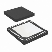
... The LMH1983 is offered in a space-saving 40- pin LLP package. Typical Application – Video Genlock Timing Generation for A/V Frame Synchronizer © 2011 National Semiconductor Corporation LMH1983 Features ■ Four PLLs for simultaneous A/V clock generation — PLL1 13.5 MHz — ...
Page 2
Functional Block Diagram www.national.com 2 30085103 ...
Page 3
Connection Diagram Ordering Information Package Part Number LMH1983SQ 40-Pin LLP LMH1983SQE LMH1983SQX Top View 40-Pin LLP (SQA40A) Transport Media 1k Units Tape and Reel 250 Units Tape and Reel 2.5k Units Tape and Reel 3 30085102 NSC Drawing SQA40A www.national.com ...
Page 4
Pin Descriptions Pin No. Pin Name – DAP 1 VDD 2 VDD 3 Hin 4 Vin 5 Fin 6 INIT 7 ADDR 8 SDA 9 SCL 10 VDD 11 NO_LOCK 12 NO_ALIGN 13 NO_REF 14 CLKout4– 15 CLKout4+ 16 VDD ...
Page 5
Pin No. Pin Name I/O 30 Fout2 O – 31 VDD – 32 VDD 33 XOin– XOin+ 35 CLKout1– CLKout1+ 37 Fout1 O – 38 VDD – 39 GND 40 VC_LPF O Notes 1. The NO_LOCK ...
Page 6
... Absolute Maximum Ratings If Military/Aerospace specified devices are required, please contact the National Semiconductor Sales Office/ Distributors for availability and specifications. ESD Tolerance (Note 2) Human Body Model Machine Model Charge-Device Model Supply Voltage Input Voltage (any input) Output Voltage (any output) Storage Temperature Range ...
Page 7
Symbol Parameter t 8) Timing output delay time (Note D1 t Timing output delay time D2 t Timing output delay time D3 t Timing output delay time D4 Video and Audio Clock Outputs (CLKout1, CLKout2 and CLKout3 MHz ...
Page 8
Symbol Parameter T Duty Cycle D t Rise Time R 20% to 80% t Fall Time F 80% to 20% V Differential Signal Output OD Voltage Common Signal Output Voltage 100Ω differential load, CLKout1, CLKout2 |Change ...
Page 9
9 www.national.com ...
Page 10
Auto Format Detection Codes The Auto Format Detection Codes apply to registers 0x07 (Output Mode – PLL2 Format), 0x08 (Output Mode – PLL3 Format) and 0x20 (Input Format). Format Code ...
Page 11
Register Descriptions The following table provides details on the device's configuration registers. Default value for fields 7 bits and less are expressed in binary, default values for fields that are 8 bits (Byte) are expressed in hex. Do not write ...
Page 12
ADD Name Bits 0x05 Device Control 4 0x06 Input Polarity 7 0x07 Output Mode – PLL2 7:6 Format 5:0 0x08 Output Mode – PLL3 7:6 Format 5:0 www.national.com Field R/W ...
Page 13
ADD Name Bits 0x09 Output Mode – Misc 7:5 4 3:0 0x0A Output Buffer Control 7:4 3:0 0x0B Output Frame Control 7:5 – Offset1_MSB 4:0 0x0C Output Frame Control 7:0 – Offset1_LSB 0x0D Output Frame Control 7:5 – Offset2_MSB 4:0 ...
Page 14
ADD Name Bits 0x11 Alignment Control – 7:6 TOF1 5 0x12 Alignment Control – 7:6 TOF2 5:4 3:1 0 www.national.com Field R/W Default RSVD TOF1_Align_Mode R/W 11 TOF1_Sync_Near R/W 1 TOF1_Sync_Far R/W 0 TOF1_Sync_Slew R/W 0 ...
Page 15
ADD Name Bits 0x13 Alignment Control – 7:6 TOF3 5:4 3:1 0 0x14 Alignment Control – 7:6 AFS 5:4 3 2:1 0 0x15 Loss of Alignment 7:3 Control 2:0 Field R/W Default RSVD TOF3_Align_Mode R/W 11 RSVD TOF3_INIT R/W 0 ...
Page 16
ADD Name Bits 0x16 LOR Control – 7:2 Holdover Sampled 1:0 Voltage MSB 0x17 LOR Control – 7:0 Holdover Sampled Voltage LSB 0x18 LOR Control Free-run 7:2 Control Voltage MSB 1:0 0x19 LOR Control – Free- 7:0 run Control Voltage ...
Page 17
ADD Name Bits 0x1B Loss of Reference 7 Threshold 6:4 3 2:0 0x1C Loss of Lock 7:5 Threshold 4:0 0x1D Mask Control – PLL 7 Lock and Output Align 0x1E Reserved 7:0 0x1F ...
Page 18
ADD Name Bits 0x22 Output Frame Lookup 7:4 – PLL2 Vsync Code 3:0 0x23 Output Frame Lookup 7:4 – PLL3 Vsync Code 3:0 0x24 Reserved 7:0 0x25 PLL1 Advanced 7:5 Control 0x26 PLL1 Advanced 7:4 ...
Page 19
ADD Name Bits 0x2B PLL1 Advanced 7 Control 6:0 N Counter MSB 0x2C PLL1 Advanced 7:0 Control N Counter LSB 0x2D PLL1 Advanced 7:5 Control 4:0 Lock Step Size 0x2E PLL2 Advanced 7:5 Control 4 Main 3 2:0 0x2F PLL2 ...
Page 20
ADD Name Bits 0x37 PLL4 Advanced 7:2 Control 1:0 N counter MSB 0x38 PLL4 Advanced 7:0 Control N counter LSB 0x39 PLL4 Advanced 7:0 Control VCO Range 0x3A LVDS Control 7 6:4 3:0 0x3B TOF1 Adv Control 7:5 LPF MSB ...
Page 21
ADD Name Bits 0x47 TOF3 Advanced 7:5 Control 4:0 Frame Reset MSB 0x48 TOF3 Advanced 7:0 Control Frame Reset LSB 0x49 TOF4 Advanced 7:0 Control AFS 0x4A TOF4 Advanced 7:4 Control 3:0 ACLK 0x4B Reserved 7:0 to 0x50 0x51 User ...
Page 22
ADD Name Bits 0x5D User Auto Format 7 Misc 6:5 4 3:0 www.national.com Field R/W Default EN_USERMODE R/W 0 RSVD USR_IINTERLACE R USR_IN_VS_CODE R/W 0000 22 Description Enables the Auto Format Detection User Mode disabled 1 ...
Page 23
Crosspoint Output Selection Table Register 0x09 [3:0] PLL2_disable 0000 (default) 0001 0010 0011 0100 0101 0110 0111 1000 1001 1010 1011 1100 1101 1110 1111 Vsync Codes Vsync codes are used by registers 0x21(Output Frame Lookup – Input Vsync Code), ...
Page 24
Application Information Functional Overview The LMH1983 is an analog phase locked loop (PLL) clock generator that can output simultaneous clocks at any of a va- riety of video and audio rates, synchronized or “genlocked” sync and V sync ...
Page 25
Initialization Under some circumstances possible for an LMH1983 to power anomalous state in which the output of PLL3 exhibits a large amount of cycle to cycle jitter. A simple reg- ister write after power up ...
Page 26
TOF1 and V pared, and depending upon the mode of the device, this loop can drive the VCXO control voltage to slew the output clocks into alignment. PLL1 Loop Response Design Equations The ...
Page 27
Loop Filter Capacitors The most common types of capacitors used in many circuits today are ferroelectric ceramic capacitors such as X7R, Y5V, X5R. Y5U, etc. These capacitors suffer from piezoelectric ef- fects, which generate an electrical signal in response to ...
Page 28
To determine the status of the NOLOCK indication, the LMH1983 sets up a window where it looks at the amount of adjustment that is required, over a period of time. Each of these two parameters is set via a register ...
Page 29
... This is the methodology DJ RJ used by the jitter analysis tools supported on high bandwidth National Semiconductor web site for detailed instructions on how to set up the appropriate register settings to generate 44.1 kHz audio clocks. TOF4 has two different modes in which it can operate. When the AFS_mode bit (in register 0x09) is set then TOF4 ...
Page 30
CLKout1 Jitter Histogram Horizontal scale: 2.6ps / division CLKout2 Jitter Histogram Horizontal scale: 4.4ps / division CLKout3 Jitter Histogram Horizontal scale: 4.4ps / div www.national.com 30085155 CLKout1 Phase Noise 30085156 CLKout2 Phase Noise 30085157 CLKout3 Phase Noise 30 30085151 30085152 ...
Page 31
CLKout4 Jitter Histogram Horizontal scale div Output Driver Adjustments The LVDS output drivers can be adjusted via the I to change the differential output voltage swing, the common mode voltage and to apply pre-emphasis to the LVDS ...
Page 32
Furthermore, if the difference is large, then the user has the opportunity to tell the device to achieve alignment either via advancing or retarding the phase of PLL1 in order to achieve alignment. Note that ...
Page 33
User Defined Formats There are several registers in the LMH1983 which are loaded automatically based on the format of the reference that is de- tected. The LMH1983 allows the user to define a non-stan- dard format, and the appropriate register ...
Page 34
One potential source of jitter on a multiple clock system such as the LMH1983 is interference between the four PLLs on the chip. To help reduce this effect, internally on the LMH1983 each PLL is run from a separate power ...
Page 35
High-Precision, Stable A/V clock generation using a 27 MHz TCXO Reference PCB Design Do's and Don'ts DO whenever possible dedicate an entire layer to each power supply. This will reduce the inductance in the supply plane. DO use surface mount ...
Page 36
Physical Dimensions www.national.com inches (millimeters) unless otherwise noted 40-Pin LLP NS Package Number SQA40A 36 ...
Page 37
Notes 37 www.national.com ...
Page 38
... For more National Semiconductor product information and proven design tools, visit the following Web sites at: www.national.com Products Amplifiers www.national.com/amplifiers Audio www.national.com/audio Clock and Timing www.national.com/timing Data Converters www.national.com/adc Interface www.national.com/interface LVDS www.national.com/lvds Power Management www.national.com/power Switching Regulators www.national.com/switchers LDOs www.national.com/ldo LED Lighting www ...