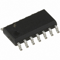
74LCX125MX Fairchild Semiconductor, 74LCX125MX Datasheet - Page 3

74LCX125MX
Manufacturer Part Number
74LCX125MX
Description
IC BUFFER QUAD LV N-INV 14SOIC
Manufacturer
Fairchild Semiconductor
Series
74LCXr
Datasheet
1.74LCX125MX.pdf
(13 pages)
Specifications of 74LCX125MX
Logic Type
Buffer/Line Driver, Non-Inverting
Number Of Elements
4
Number Of Bits Per Element
1
Current - Output High, Low
24mA, 24mA
Voltage - Supply
2 V ~ 3.6 V
Operating Temperature
-40°C ~ 85°C
Mounting Type
Surface Mount
Package / Case
14-SOIC (3.9mm Width), 14-SOL
Logic Family
LCX
Number Of Channels Per Chip
4
Polarity
Non-Inverting
Supply Voltage (max)
3.6 V
Supply Voltage (min)
2 V
Maximum Operating Temperature
+ 85 C
Mounting Style
SMD/SMT
High Level Output Current
- 24 mA
Low Level Output Current
24 mA
Maximum Power Dissipation
25 pF
Minimum Operating Temperature
- 40 C
Number Of Lines (input / Output)
4 / 4
Output Type
3-State
Propagation Delay Time
6.5 ns at 2.7 V, 6 ns at 3.3 V
Logical Function
Buffer/Line Driver
Number Of Elements
4
Number Of Channels
4
Number Of Inputs
4
Number Of Outputs
4
Operating Supply Voltage (typ)
2.5/3.3V
Package Type
SOIC N
Operating Supply Voltage (max)
3.6V
Operating Supply Voltage (min)
2V
Quiescent Current
10uA
Technology
CMOS
Pin Count
14
Mounting
Surface Mount
Operating Temp Range
-40C to 85C
Operating Temperature Classification
Industrial
Dc
0406
Lead Free Status / RoHS Status
Lead free / RoHS Compliant
Other names
74LCX125MXTR
Available stocks
Company
Part Number
Manufacturer
Quantity
Price
Company:
Part Number:
74LCX125MX
Manufacturer:
FAIRCHIL
Quantity:
3 321
Part Number:
74LCX125MX
Manufacturer:
FAIRCHILD/仙童
Quantity:
20 000
©1995 Fairchild Semiconductor Corporation
74LCX125 Rev. 1.7.0
Absolute Maximum Ratings
Stresses exceeding the absolute maximum ratings may damage the device. The device may not function or be
operable above the recommended operating conditions and stressing the parts to these levels is not recommended.
In addition, extended exposure to stresses above the recommended operating conditions may affect device reliability.
The absolute maximum ratings are stress ratings only.
Note:
3. I
Recommended Operating Conditions
The Recommended Operating Conditions table defines the conditions for actual device operation. Recommended
operating conditions are specified to ensure optimal performance to the datasheet specifications. Fairchild does not
recommend exceeding them or designing to absolute maximum ratings.
Note:
4. Unused inputs must be held HIGH or LOW. They may not float.
Symbol
Symbol
I
O
OH
T
I
V
V
t / V
I
GND
I
Absolute Maximum Rating must be observed.
V
V
I
STG
T
V
OK
I
CC
V
CC
IK
CC
O
/ I
O
O
A
I
I
OL
Supply Voltage
DC Input Voltage
DC Output Voltage,
DC Input Diode Current, V
DC Output Diode Current
DC Output Source/Sink Current
DC Supply Current per Supply Pin
DC Ground Current per Ground Pin
Storage Temperature
Supply Voltage
Input Voltage
Output Voltage
Output Current
Free-Air Operating Temperature
Input Edge Rate, V
Output in 3-STATE
Output in HIGH or LOW State
V
V
Operating
Data Retention
HIGH or LOW State
3-STATE
V
V
V
O
O
CC
CC
CC
V
GND
CC
3.0V–3.6V
2.7V–3.0V
2.3V–2.7V
IN
0.8V–2.0V, V
Parameter
I
GND
Parameter
(3)
CC
(4)
3.0V
3
Min.
–40
2.0
1.5
0
0
0
0
Max.
V
±24
±12
3.6
3.6
5.5
5.5
–0.5V to V
±8
85
10
CC
Rating
–65°C to +150°C
–0.5V to +7.0V
–0.5V to +7.0V
–0.5V to +7.0V
www.fairchildsemi.com
CC
±100mA
±100mA
Units
ns / V
–50mA
–50mA
+50mA
±50mA
mA
°C
+ 0.5V
V
V
V


