M74VHC1GT126DF1G ON Semiconductor, M74VHC1GT126DF1G Datasheet
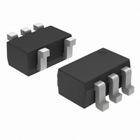
IC BUFF CMOS LVL/SFTR N-I SOT353

M74VHC1GT126DF1G

Manufacturer Part Number
M74VHC1GT126DF1G
Description
IC BUFF CMOS LVL/SFTR N-I SOT353
Manufacturer
ON Semiconductor
Series
74VHCr
Datasheet

Specifications of M74VHC1GT126DF1G

Logic Type
Buffer/Line Driver, Non-Inverting
Number Of Elements
1
Number Of Bits Per Element
1
Current - Output High, Low
8mA, 8mA
Voltage - Supply
3 V ~ 5.5 V
Operating Temperature
-55°C ~ 125°C
Mounting Type
Surface Mount
Package / Case
SC-70-5, SC-88A, SOT-323-5, SOT-353, 5-TSSOP
Logic Family
74VHC
Number Of Channels Per Chip
Single
Polarity
Non-Inverting
Supply Voltage (max)
5.5 V
Supply Voltage (min)
3 V
Maximum Operating Temperature
125 C
Mounting Style
SMD/SMT
High Level Output Current
- 8 mA
Input Bias Current (max)
1 uA
Low Level Output Current
8 mA
Maximum Power Dissipation
200 mW
Minimum Operating Temperature
- 55 C
Number Of Lines (input / Output)
3
Output Type
3-State
Propagation Delay Time
11.5 ns @ 3.3 V or 7.5 ns @ 5 V
Logical Function
Buffer/Line Driver
Number Of Elements
1
Number Of Channels
1
Number Of Inputs
1
Number Of Outputs
1
Operating Supply Voltage (typ)
3.3/5V
Package Type
SC-70
Operating Supply Voltage (max)
5.5V
Operating Supply Voltage (min)
3V
Quiescent Current
1uA
Technology
CMOS
Pin Count
5
Mounting
Surface Mount
Operating Temp Range
-55C to 125C
Operating Temperature Classification
Military
Logic Device Type
Buffer, Non Inverting
Supply Voltage Range
3V To 5.5V
Logic Case Style
SOT-353
No. Of Pins
5
Operating Temperature Range
-55°C To +125°C
Filter Terminals
SMD
Rohs Compliant
Yes
Family Type
VHC
Lead Free Status / RoHS Status
Lead free / RoHS Compliant
Other names
M74VHC1GT126DF1G
M74VHC1GT126DF1GOSTR

Available stocks

Company
Part Number
Manufacturer
Quantity
Price
Part Number:
M74VHC1GT126DF1G
Manufacturer:
ON Semiconductor
Quantity:
12 500
Part Number:
M74VHC1GT126DF1G
Manufacturer:
ON/安森美
Quantity:
20 000
Part Number:
M74VHC1GT126DF1G
Manufacturer:
ON
Quantity:
15 575
Part Number:
M74VHC1GT126DF1G
0
Company:
Part Number:
M74VHC1GT126DF1G
Quantity:
3 000
MC74VHC1GT126
Noninverting Buffer /
CMOS Logic Level Shifter
with LSTTL−Compatible Inputs
fabricated with silicon gate CMOS technology. It achieves high speed
operation similar to equivalent Bipolar Schottky TTL while maintaining
CMOS low power dissipation.
set Low to place the output into the high impedance state.
the output has a full 5 V CMOS level output swing. The input
protection circuitry on this device allows overvoltage tolerance on the
input, allowing the device to be used as a logic−level translator from
3 V CMOS logic to 5 V CMOS Logic or from 1.8 V CMOS logic to
3 V CMOS Logic while operating at the high−voltage power supply.
voltages up to 7 V are applied, regardless of the supply voltage. This
allows the MC74VHC1GT126 to be used to interface 5 V circuits to
3 V circuits. The output structures also provide protection when
V
destruction caused by supply voltage − input/output voltage mismatch,
battery backup, hot insertion, etc.
Features
© Semiconductor Components Industries, LLC, 2007
February, 2007 − Rev. 13
CC
The MC74VHC1GT126 is a single gate noninverting 3−state buffer
The MC74VHC1GT126 requires the 3−state control input (OE) to be
The device input is compatible with TTL−type input thresholds and
The MC74VHC1GT126 input structure provides protection when
CMOS−Compatible Outputs: V
High Speed: t
Low Power Dissipation: I
TTL−Compatible Inputs: V
Power Down Protection Provided on Inputs and Outputs
Balanced Propagation Delays
Pin and Function Compatible with Other Standard Logic Families
Chip Complexity: FETs = 62; Equivalent Gates = 16
Pb−Free Packages are Available
= 0 V. These input and output structures help prevent device
PD
IN A
OE
= 3.5 ns (Typ) at V
GND
Figure 1. Pinout (Top View)
IN A
OE
Figure 2. Logic Symbol
1
2
3
CC
IL
= 1 mA (Max) at T
= 0.8 V; V
OH
> 0.8 V
CC
5
4
= 5 V
IH
CC
V
OUT Y
CC
= 2 V
; V
OUT Y
OL
A
= 25°C
< 0.1 V
CC
1
@Load
See detailed ordering and shipping information in the package
dimensions section on page 4 of this data sheet.
SC−88A/SOT−353/SC−70
*Date Code orientation and/or position may vary
TSOP−5/SOT−23/SC−59
depending upon manufacturing location.
A Input
(Note: Microdot may be in either location)
1
2
4
3
5
H
X
L
CASE 419A
5
DF SUFFIX
DT SUFFIX
CASE 483
ORDERING INFORMATION
5
W3
M
G
http://onsemi.com
1
FUNCTION TABLE
PIN ASSIGNMENT
1
= Device Code
= Date Code*
= Pb−Free Package
OE Input
H
H
L
Publication Order Number:
OUT Y
GND
MC74VHC1GT126/D
IN A
V
OE
CC
5
DIAGRAMS
1
5
1
MARKING
Y Output
W3 M G
W3 M G
H
L
Z
G
G

Related parts for M74VHC1GT126DF1G

M74VHC1GT126DF1G Summary of contents

Page 1

MC74VHC1GT126 Noninverting Buffer / CMOS Logic Level Shifter with LSTTL−Compatible Inputs The MC74VHC1GT126 is a single gate noninverting 3−state buffer fabricated with silicon gate CMOS technology. It achieves high speed operation similar to equivalent Bipolar Schottky TTL while maintaining CMOS ...

Page 2

MAXIMUM RATINGS Symbol V DC Supply Voltage Input Voltage Output Voltage OUT I Input Diode Current IK I Output Diode Current Output Current, per Pin OUT I DC Supply Current, V ...

Page 3

DC ELECTRICAL CHARACTERISTICS Î Î Î Î ...

Page 4

... TEST *Includes all probe and jig capacitance Figure 6. Test Circuit ORDERING INFORMATION Device MC74VHC1GT126DF1 M74VHC1GT126DF1G MC74VHC1GT126DF2 M74VHC1GT126DF2G MC74VHC1GT126DT1 M74VHC1GT126DT1G †For information on tape and reel specifications, including part orientation and tape sizes, please refer to our Tape and Reel Packaging Specifications Brochure, BRD8011/D. ...

Page 5

... C H SOLDERING FOOTPRINT* 0.50 0.0197 0.40 0.0157 *For additional information on our Pb−Free strategy and soldering details, please download the ON Semiconductor Soldering and Mounting Techniques Reference Manual, SOLDERRM/D. MC74VHC1GT126 SC−88A, SOT−353, SC−70 CASE 419A−02 ISSUE J NOTES: 1. DIMENSIONING AND TOLERANCING PER ANSI Y14.5M, 1982. ...

Page 6

... H T *For additional information on our Pb−Free strategy and soldering details, please download the ON Semiconductor Soldering and Mounting Techniques Reference Manual, SOLDERRM/D. ON Semiconductor and are registered trademarks of Semiconductor Components Industries, LLC (SCILLC). SCILLC reserves the right to make changes without further notice to any products herein. SCILLC makes no warranty, representation or guarantee regarding the suitability of its products for any particular purpose, nor does SCILLC assume any liability arising out of the application or use of any product or circuit, and specifically disclaims any and all liability, including without limitation special, consequential or incidental damages. “ ...

Related keywords