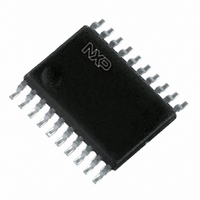
74LVC273PW,118 NXP Semiconductors, 74LVC273PW,118 Datasheet - Page 2

74LVC273PW,118
Manufacturer Part Number
74LVC273PW,118
Description
IC OCT D-TYPE FLIP-FLOP 20TSSOP
Manufacturer
NXP Semiconductors
Series
74LVCr
Type
D-Type Busr
Datasheet
1.74LVC273PW118.pdf
(18 pages)
Specifications of 74LVC273PW,118
Package / Case
20-TSSOP
Function
Master Reset
Output Type
Non-Inverted
Number Of Elements
1
Number Of Bits Per Element
8
Frequency - Clock
150MHz
Delay Time - Propagation
1.5ns
Trigger Type
Positive Edge
Current - Output High, Low
24mA, 24mA
Voltage - Supply
2.7 V ~ 3.6 V
Operating Temperature
-40°C ~ 125°C
Mounting Type
Surface Mount
Number Of Circuits
1
Logic Family
LVC
Logic Type
D-Type Edge Triggered Flip-Flop
Polarity
Non-Inverting
Input Type
Single-Ended
Propagation Delay Time
6 ns at 3.3 V
High Level Output Current
- 24 mA
Supply Voltage (max)
3.6 V
Maximum Operating Temperature
+ 125 C
Mounting Style
SMD/SMT
Minimum Operating Temperature
- 40 C
Supply Voltage (min)
1.2 V
Lead Free Status / RoHS Status
Lead free / RoHS Compliant
Lead Free Status / RoHS Status
Lead free / RoHS Compliant, Lead free / RoHS Compliant
Other names
568-2268-2
74LVC273PW-T
935210650118
74LVC273PW-T
935210650118
Available stocks
Company
Part Number
Manufacturer
Quantity
Price
Company:
Part Number:
74LVC273PW,118
Manufacturer:
NXP Semiconductors
Quantity:
1 950
Part Number:
74LVC273PW,118
Manufacturer:
NXP/恩智浦
Quantity:
20 000
Philips Semiconductors
FEATURES
QUICK REFERENCE DATA
GND = 0 V; T
Notes
1. C
2. The definition is V
2004 Mar 12
t
f
C
C
PHL
max
SYMBOL
Wide supply voltage range from 1.2 to 3.6 V
Inputs accept voltages up to 5.5 V
CMOS low power consumption
Direct interface with TTL levels
Output drive capability 50
Complies with JEDEC standard no. 8-1A
ESD protection:
HBM EIA/JESD22-A114-A exceeds 2000 V
MM EIA/JESD22-A115-A exceeds 200 V.
Specified from 40 to +85 C and 40 to +125 C.
I
PD
Octal D-type flip-flop with reset;
positive-edge trigger
P
f
f
C
V
N = total load switching outputs;
i
o
/t
(C
D
CC
PD
= input frequency in MHz;
L
PLH
= output frequency in MHz;
= output load capacitance in pF;
= C
L
is used to determine the dynamic power dissipation (P
= supply voltage in Volts;
PD
V
CC
amb
propagation delay CP to Qn
propagation delay MR to Qn
maximum clock frequency
input capacitance
power dissipation capacitance per flip-flop
2
V
CC
= 25 C; t
f
o
2
) = sum of the outputs.
I
f
= GND to V
i
N + (C
r
= t
PARAMETER
f
transmission lines at 85 C
2.5 ns.
L
CC
.
V
CC
2
f
o
) where:
2
C
C
outputs disabled; notes 1 and 2 22
L
L
DESCRIPTION
The 74LVC273 is a low-voltage Si-gate CMOS device,
superior to most advanced CMOS compatible TTL
families.
The 74LVC273 has eight edge-triggered, D-type flip-flops
with individual D inputs and Q outputs. The common clock
(CP) and master reset (MR) inputs load and reset (clear)
all flip-flops simultaneously. The state of each D input, one
set-up time before the LOW-to-HIGH clock transition, is
transferred to the corresponding output (Qn) of the
flip-flop.
All outputs will be forced LOW independently of clock or
data inputs by a LOW voltage level on the MR input.
The device is useful for applications where the true output
only is required and the clock and master reset are
common to all storage elements.
= 50 pF; V
= 50 pF; V
D
in W)
CONDITIONS
CC
CC
= 3.3 V
= 3.3 V
4.8
4.8
230
5.0
TYPICAL
Product specification
74LVC273
ns
ns
MHz
pF
pF
UNIT


