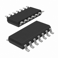
HEF4013BT,652 NXP Semiconductors, HEF4013BT,652 Datasheet - Page 12

HEF4013BT,652
Manufacturer Part Number
HEF4013BT,652
Description
IC FLIP FLOP DUAL D TYPE 14SOIC
Manufacturer
NXP Semiconductors
Series
4000Br
Type
D-Typer
Specifications of HEF4013BT,652
Package / Case
14-SOIC (3.9mm Width), 14-SOL
Function
Set(Preset) and Reset
Output Type
Differential
Number Of Elements
2
Number Of Bits Per Element
1
Frequency - Clock
40MHz
Trigger Type
Positive Edge
Current - Output High, Low
3.4mA, 3.4mA
Voltage - Supply
3 V ~ 15 V
Operating Temperature
-40°C ~ 125°C
Mounting Type
Surface Mount
Number Of Circuits
2
Logic Family
HE4000B
Logic Type
D-Type Flip-Flop
Polarity
Inverting/Non-Inverting
Input Type
Single-Ended
Propagation Delay Time
90 ns
High Level Output Current
- 4.2 mA
Low Level Output Current
4.2 mA
Supply Voltage (max)
15 V
Maximum Operating Temperature
+ 85 C
Mounting Style
SMD/SMT
Minimum Operating Temperature
- 40 C
Supply Voltage (min)
3 V
Technology
CMOS
Number Of Bits
2
Number Of Elements
2
Clock-edge Trigger Type
Positive-Edge
Operating Supply Voltage (typ)
3.3/5/9/12V
Package Type
SO
Frequency (max)
40MHz
Operating Supply Voltage (min)
3V
Operating Supply Voltage (max)
15V
Operating Temp Range
-40C to 125C
Operating Temperature Classification
Automotive
Mounting
Surface Mount
Pin Count
14
Lead Free Status / RoHS Status
Lead free / RoHS Compliant
Delay Time - Propagation
-
Lead Free Status / Rohs Status
Lead free / RoHS Compliant
Other names
568-1685-5
933372660652
HEF4013BTD
933372660652
HEF4013BTD
Philips Semiconductors
DEFINITIONS OF SYMBOLS AND TERMS USED IN
DATA SHEETS
Currents
Positive current is defined as conventional current flow
into a device.
Negative current is defined as conventional current flow
out of a device.
January 1995
I
I
I
I
I
I
I
I
I
I
IN
OH
OL
DD
OZ
IL
IH
DDL
DDH
Z
Input current; the current flowing into a device
at specified input voltage and V
Output current HIGH; the drive current flowing
out of a device at specified HIGH output voltage
and V
Output current LOW; the drive current flowing
into a device at specified LOW output voltage
and V
Quiescent power supply current; the current
flowing into the V
V
Output OFF current; the leakage current
flowing into or out of the output of a 3-state
device in the OFF state when the output is
connected to V
Input current LOW; the current flowing into a
device at a specified LOW level input voltage
and a specified V
Input current HIGH; the current flowing into a
device at a specified HIGH level input voltage
and a specified V
Quiescent power supply current LOW; the
current flowing into the V
specified LOW level input voltage on all inputs
and specified V
Quiescent power supply current HIGH; the
current flowing into the V
specified HIGH level input voltage on all inputs
and specified V
OFF state leakage current; the leakage current
flowing into the output of a 3-state device in the
OFF state at a specified output voltage and
V
DD
DD
.
conditions.
DD
DD
.
.
DD
DD
DD
DD
DD
DD
or V
conditions.
conditions.
.
.
lead at specified input and
SS
.
DD
DD
lead with a
lead with a
DD
.
12
Voltages
All voltages are referenced to V
negative potential applied to the device.
Analogue terms
V
V
V
V
V
V
V
V
V
R
DD
SS
EE
IH
IL
OH
OL
P
N
R
ON
ON
Supply voltage; the most positive potential on
the device.
Supply voltage; for a device with a single
negative power supply, the most negative
power supply, used as the reference level for
other voltages; typically ground.
Supply voltage; one of two (V
negative power supplies. For a device with dual
negative power supply, the most negative
power supply as a reference level for other
voltages.
Input voltage HIGH; the range of input voltages
that represents a logic HIGH level in the
system.
Input voltage LOW; the range of input voltages
that represents a logic LOW level in the system.
Output voltage HIGH; the range of voltages at
an output terminal with a specified output
loading and supply voltage. Device inputs are
conditioned to establish a HIGH level at the
output.
Output voltage LOW; the range of voltages at
an output terminal with a specified output
loading and supply voltage. Device inputs are
conditioned to establish a LOW level at the
output.
Trigger threshold voltage; positive-going signal.
Trigger threshold voltage; negative-going
signal.
ON resistance; the effective ON state
resistance of an analogue transmission gate, at
specified input voltage, output load and V
resistance between any two transmission gates
of an analogue device at specified input
voltage, output load and V
ON resistance; the difference in effective ON
Family Specifications
SS
, which is the most
DD
.
SS
and V
EE
)
DD
.


