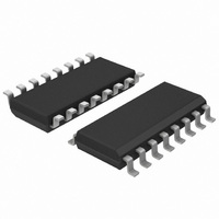
74HC4049D,653 NXP Semiconductors, 74HC4049D,653 Datasheet - Page 2

74HC4049D,653
Manufacturer Part Number
74HC4049D,653
Description
IC HEX INV LEVEL SHIFTER 16SOIC
Manufacturer
NXP Semiconductors
Series
74HCr
Datasheet
1.74HC4049DB112.pdf
(15 pages)
Specifications of 74HC4049D,653
Logic Type
Inverter
Number Of Inputs
1
Number Of Circuits
6
Current - Output High, Low
5.2mA, 5.2mA
Voltage - Supply
2 V ~ 6 V
Mounting Type
Surface Mount
Package / Case
16-SOIC (3.9mm Width)
Logic Family
HC
Number Of Channels Per Chip
6
Polarity
Inverting
Supply Voltage (max)
6 V
Supply Voltage (min)
2 V
Maximum Operating Temperature
+ 125 C
Mounting Style
SMD/SMT
High Level Output Current
- 5.2 mA
Low Level Output Current
5.2 mA
Minimum Operating Temperature
- 40 C
Number Of Lines (input / Output)
6 / 6
Propagation Delay Time
85 ns at 2 V, 17 ns at 4.5 V, 14 ns at 6 V
Lead Free Status / RoHS Status
Lead free / RoHS Compliant
Operating Temperature
-
Lead Free Status / Rohs Status
Details
Other names
74HC4049D-T
74HC4049D-T
933714800653
74HC4049D-T
933714800653
NXP Semiconductors
4. Functional diagram
5. Pinning information
74HC4049
Product data sheet
Fig 1.
Fig 4.
Logic symbol
Pin configuration DIP16 and SO16
1A
2A
3A
4A
5A
6A
3
5
7
9
11
14
GND
V
5.1 Pinning
CC
1Y
1A
2Y
2A
3Y
3A
001aai331
1
2
3
4
5
6
7
8
10
12
15
2
4
6
74HC4049
1Y
2Y
3Y
4Y
5Y
6Y
001aan372
16
15
14
13
12
11
10
9
n.c.
6Y
6A
n.c.
5Y
5A
4Y
4A
All information provided in this document is subject to legal disclaimers.
Fig 2.
Rev. 3 — 30 December 2010
11
14
3
5
7
9
IEC logic symbol
V1/V2
V1/V2
V1/V2
V1/V2
V1/V2
V1/V2
001aan374
Fig 5.
2
4
6
10
12
15
Pin configuration SSOP16 and TSSOP16
GND
V
CC
1Y
1A
2Y
2A
3Y
3A
Hex inverting HIGH-to-LOW level shifter
1
2
3
4
5
6
7
8
Fig 3.
74HC4049
A
Logic diagram (one level
shifter)
001aan373
74HC4049
© NXP B.V. 2010. All rights reserved.
16
15
14
13
12
11
10
9
n.c.
6Y
6A
n.c.
5Y
5A
4Y
4A
mna341
Y
2 of 15


