MC10H117P ON Semiconductor, MC10H117P Datasheet
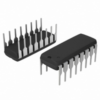
IC GATE OR/AND DUAL ECL 16-DIP

MC10H117P

Manufacturer Part Number
MC10H117P
Description
IC GATE OR/AND DUAL ECL 16-DIP
Manufacturer
ON Semiconductor
Series
10Hr
Datasheet

Specifications of MC10H117P

Logic Type
AND/OR/INVERT Gate
Number Of Circuits
2
Number Of Inputs
8 Input (2, 2, 2, 2)
Schmitt Trigger Input
No
Output Type
Differential
Operating Temperature
0°C ~ 75°C
Mounting Type
Through Hole
Package / Case
16-DIP (0.300", 7.62mm)
Lead Free Status / RoHS Status
Contains lead / RoHS non-compliant
Voltage - Supply
-
Current - Output High, Low
-
MC10H117
Dual 2−Wide 2−3−Input
OR−AND/OR−AND Gate
Description
OR−AND−Invert gate is a general purpose logic element designed for
use in data control, such as digital multiplexing or data distribution.
Pin 9 is common to both gates. This MECL 10H™ part is a
functional/pinout duplication of the standard MECL 10K™ family
part, with 100% improvement in propagation delay, and no increase in
power−supply current.
Features
*For additional information on our Pb−Free strategy and soldering details, please
© Semiconductor Components Industries, LLC, 2006
February, 2006 − Rev. 7
download the ON Semiconductor Soldering and Mounting Techniques
Reference Manual, SOLDERRM/D.
T h e M C 1 0 H 11 7 d u a l 2 −w i d e 2 −3 −i n p u t O R −A N D /
Temperature Range)
Propagation Delay, 1.0 ns Typical
Power Dissipation 100 mW/Gate Typical (same as MECL 10K)
Improved Noise Margin 150 mV (Over Operating Voltage and
Voltage Compensated
MECL 10K Compatible
Pb−Free Packages are Available*
1
See detailed ordering and shipping information in the package
dimensions section on page 3 of this data sheet.
16
20 1
*For additional marking information, refer to
CASE 620A
SOEIAJ−16
FN SUFFIX
Application Note AND8002/D.
CASE 648
CASE 966
CASE 775
1
P SUFFIX
L SUFFIX
PLLC−20
CDIP−16
PDIP−16
A
WL, L
YY, Y
WW, W = Work Week
G
ORDERING INFORMATION
http://onsemi.com
= Assembly Location
= Wafer Lot
= Year
= Pb−Free Package
16
MARKING DIAGRAMS*
1
Publication Order Number:
16
1
MC10H117L
AWLYYWW
AWLYYWW
AWLYYWWG
MC10H117P
10H117G
ALYWG
10H117
1 20
MC10H117/D

Related parts for MC10H117P

MC10H117P Summary of contents

Page 1

... Pb−Free Package *For additional marking information, refer to Application Note AND8002/D. ORDERING INFORMATION See detailed ordering and shipping information in the package dimensions section on page 3 of this data sheet MC10H117L AWLYYWW 1 MC10H117P AWLYYWWG 10H117 ALYWG 1 20 10H117G AWLYYWW Publication Order Number: MC10H117/D ...

Page 2

V = PIN 1 CC1 V = PIN 16 CC2 V = PIN 8 EE Figure 1. Logic Diagram Table 1. MAXIMUM RATINGS Symbol V Power Supply ( ...

Page 3

... MC10H117FN MC10H117FNG MC10H117FNR2 MC10H117FNR2G MC10H117L MC10H117M MC10H117MG MC10H117MEL MC10H117MELG MC10H117P MC10H117PG †For information on tape and reel specifications, including part orientation and tape sizes, please refer to our Tape and Reel Packaging Specifications Brochure, BRD8011/D. 0° 25° Min Max Min Max 0.45 1.35 ...

Page 4

Y BRK −L− −M− 0.007 (0.180) Z 0.007 (0.180 −T− J VIEW S G1 0.010 (0.250) T L− NOTES: 1. DIMENSIONS AND TOLERANCING PER ANSI Y14.5M, ...

Page 5

VIEW 0.10 (0.004) 0.13 (0.005 0.25 (0.010) PACKAGE DIMENSIONS SOEIAJ−16 CASE 966−01 ISSUE ...

Page 6

... American Technical Support: 800−282−9855 Toll Free USA/Canada Japan: ON Semiconductor, Japan Customer Focus Center 2−9−1 Kamimeguro, Meguro−ku, Tokyo, Japan 153−0051 Phone: 81−3−5773−3850 http://onsemi.com 6 NOTES: 1. DIMENSIONING AND TOLERANCING PER ANSI Y14.5M, 1982. 2. CONTROLLING DIMENSION: INCH. ...

Related keywords