M74HC259RM13TR STMicroelectronics, M74HC259RM13TR Datasheet
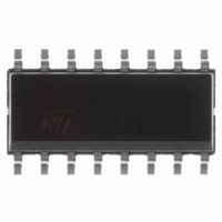
IC ADDRESSABLE LATCH 8BIT 16SOIC

M74HC259RM13TR

Manufacturer Part Number
M74HC259RM13TR
Description
IC ADDRESSABLE LATCH 8BIT 16SOIC
Manufacturer
STMicroelectronics
Series
74HCr
Datasheet

Specifications of M74HC259RM13TR

Logic Type
D-Type, Addressable
Circuit
1:8
Output Type
Standard
Voltage - Supply
2 V ~ 6 V
Independent Circuits
1
Delay Time - Propagation
15ns
Current - Output High, Low
5.2mA, 5.2mA
Operating Temperature
-55°C ~ 125°C
Mounting Type
Surface Mount
Package / Case
16-SOIC (3.9mm Width)
Lead Free Status / RoHS Status
Lead free / RoHS Compliant
Other names
497-7362-2
M74HC259RM13TR

Available stocks

Company
Part Number
Manufacturer
Quantity
Price
Part Number:
M74HC259RM13TR
Manufacturer:
SAMSUNG
Quantity:
52
Part Number:
M74HC259RM13TR
Manufacturer:
ST
0
Part Number:
M74HC259RM13TR
Manufacturer:
ST
Quantity:
20 000
Part Number:
M74HC259RM13TR
Manufacturer:
ST
Quantity:
14 028
DESCRIPTION
The M74HC259 is an high speed CMOS 8 BIT
ADDRESSABLE LATCH fabricated with silicon
gate C
The M74HC259 has single data input (D) 8 latch
outputs (Q0-Q7), 3 address inputs (A, B, and C),
common enable input (E), and a common CLEAR
input. To operate this device as an addressable
latch, data is held on the D input, and the address
of the latch into which the data is to be entered is
held on the A, B, and C inputs. When ENABLE is
taken low the data flows through to the addresses
output. The data is stored on the positive-going
edge of the ENABLE pulse. All unaddressed
latches will remain unaffected. With ENABLE in
the high state the device is deselected and all
PIN CONNECTION AND IEC LOGIC SYMBOLS
July 2001
HIGH SPEED :
t
LOW POWER DISSIPATION:
I
HIGH NOISE IMMUNITY:
V
SYMMETRICAL OUTPUT IMPEDANCE:
|I
BALANCED PROPAGATION DELAYS:
t
WIDE OPERATING VOLTAGE RANGE:
V
PIN AND FUNCTION COMPATIBLE WITH
74 SERIES 259
PD
CC
PLH
OH
NIH
CC
= 20 ns (TYP.) at V
=4 A(MAX.) at T
| = I
2
(OPR) = 2V to 6V
MOS technology.
= V
t
PHL
OL
NIL
= 4mA (MIN)
= 28 % V
A
CC
=25°C
CC
(MIN.)
= 6V
8 BIT ADDRESSABLE LATCH
ORDER CODES
latches remain in their previous state, unaffected
by changes on the data or address inputs. To
eliminate the possibility of entering erroneous data
into the latches, the ENABLE should be held high
(inactive) while the address lines are changing. If
ENABLE is held high and CLEAR is taken low all
eight latches are cleared to the low state. If
ENABLE is low all latches except the addressed
latch will be cleared. The addressed latch will
instead
implementing a 3-to-8 line decoder.
All inputs are equipped with protection circuits
against static discharge and transient excess
voltage.
PACKAGE
TSSOP
SOP
DIP
DIP
follow
M74HC259M1R
M74HC259B1R
TUBE
the
SOP
D
M74HC259
M74HC259RM13TR
input,
M74HC259TTR
T & R
TSSOP
effectively
1/13

Related parts for M74HC259RM13TR

M74HC259RM13TR Summary of contents

Page 1

... ENABLE is low all latches except the addressed latch will be cleared. The addressed latch will instead follow the D implementing a 3-to-8 line decoder. All inputs are equipped with protection circuits against static discharge and transient excess voltage. TSSOP T & R M74HC259RM13TR M74HC259TTR input, effectively 1/13 ...

Page 2

M74HC259 INPUT AND OUTPUT EQUIVALENT CIRCUIT TRUTH TABLE INPUTS ADDRESSED LATCH CLEAR ENABLE The level at the data input Qi0 : The level before the indicated steady state input conditions ...

Page 3

LOGIC DIAGRAM This logic diagram has not be used to estimate propagation delays ABSOLUTE MAXIMUM RATINGS Symbol V Supply Voltage Input Voltage Output Voltage Input Diode Current Output ...

Page 4

M74HC259 RECOMMENDED OPERATING CONDITIONS Symbol V Supply Voltage CC V Input Voltage I V Output Voltage O T Operating Temperature op Input Rise and Fall Time SPECIFICATIONS Symbol Parameter V V High Level Input ...

Page 5

AC ELECTRICAL CHARACTERISTICS (C Symbol Parameter Output Transition TLH THL Time t t Propagation Delay PLH PHL Time (DATA - Propagation Delay PLH PHL Time ( Propagation Delay ...

Page 6

M74HC259 TEST CIRCUIT C = 50pF or equivalent (includes jig and probe capacitance pulse generator (typically OUT WAVEFORM 1: PROPAGATION DELAY TIME (f=1MHz; 50% duty cycle) 6/13 ...

Page 7

WAVEFORM 2 : PROPAGATION DELAY TIME (f=1MHz; 50% duty cycle) WAVEFORM 3 : MINIMUM PULSE WIDTH (G), SETUP AND HOLD TIME (D TO G)(f=1MHz; 50% duty cycle) M74HC259 7/13 ...

Page 8

M74HC259 WAVEFORM 4 : MINIMUM PULSE WIDTH (CLR) (f=1MHz; 50% duty cycle) WAVEFORM 5 : SETUP AND HOLD TIME (f=1MHz; 50% duty cycle) 8/13 ...

Page 9

WAVEFORM 6 : INPUT WAVEFORMS (f=1MHz; 50% duty cycle) M74HC259 9/13 ...

Page 10

M74HC259 DIM. MIN. a1 0. 10/13 Plastic DIP-16 (0.25) MECHANICAL DATA mm. TYP MAX. 1.65 0.5 0.25 20 8.5 2.54 17.78 7.1 5.1 3.3 1.27 inch MIN. TYP. ...

Page 11

SO-16 MECHANICAL DATA mm. DIM. MIN 0 0. 9 3.8 G 4 TYP MAX. MIN. 1.75 0.2 0.003 1.65 0.46 0.013 0.25 ...

Page 12

M74HC259 DIM. MIN 0.05 A2 0.8 b 0.19 c 0.09 D 4.9 E 6 0° PIN 1 IDENTIFICATION 1 12/13 TSSOP16 MECHANICAL DATA mm. TYP MAX. 1.2 0.15 ...

Page 13

... No license is granted by implication or otherwise under any patent or patent rights of STMicroelectronics. Specifications mentioned in this publication are subject to change without notice. This publication supersedes and replaces all information previously supplied ...

Related keywords