MM74HC165N Fairchild Semiconductor, MM74HC165N Datasheet

IC REGIST PAR-IN/SER-OUT 16-DIP

MM74HC165N

Manufacturer Part Number
MM74HC165N
Description
IC REGIST PAR-IN/SER-OUT 16-DIP
Manufacturer
Fairchild Semiconductor
Series
74HCr
Datasheet

Specifications of MM74HC165N

Logic Type
Shift Register
Output Type
Differential
Number Of Elements
1
Number Of Bits Per Element
8
Function
Parallel or Serial to Serial
Voltage - Supply
2 V ~ 6 V
Operating Temperature
-40°C ~ 85°C
Mounting Type
Through Hole
Package / Case
16-DIP (0.300", 7.62mm)
Counting Sequence
Serial/Parallel to Serial
Number Of Circuits
1
Logic Family
74HC
Propagation Delay Time
150 ns, 30 ns, 26 ns
Supply Voltage (max)
6 V
Maximum Operating Temperature
+ 85 C
Minimum Operating Temperature
- 40 C
Mounting Style
Through Hole
Operating Supply Voltage
2 V to 6 V
Shift Register Function
Parallel To Serial
No. Of Elements
1
Ic Output Type
Differential
Logic Case Style
DIP
No. Of Pins
16
Supply Voltage Range
2V To 6V
Rohs Compliant
Yes
Lead Free Status / RoHS Status
Lead free / RoHS Compliant
Other names
74HC165

Available stocks

Company
Part Number
Manufacturer
Quantity
Price
Part Number:
MM74HC165N
Manufacturer:
NS/国半
Quantity:
20 000
© 1999 Fairchild Semiconductor Corporation
MM74HC165M
MM74HC165SJ
MM74HC165MTC
MM74HC165
MM74HC165
Parallel-in/Serial-out 8-Bit Shift Register
General Description
The MM74HC165 high speed PARALLEL-IN/SERIAL-OUT
SHIFT REGISTER utilizes advanced silicon-gate CMOS
technology. It has the low power consumption and high
noise immunity of standard CMOS integrated circuits,
along with the ability to drive 10 LS-TTL loads.
This 8-bit serial shift register shifts data from Q
when clocked. Parallel inputs to each stage are enabled by
a low level at the SHIFT/LOAD input. Also included is a
gated CLOCK input and a complementary output from the
eighth bit.
Clocking is accomplished through a 2-input NOR gate per-
mitting one input to be used as a CLOCK INHIBIT function.
Holding either of the CLOCK inputs high inhibits clocking,
and holding either CLOCK input low with the SHIFT/LOAD
input high enables the other CLOCK input. Data transfer
occurs on the positive going edge of the clock. Parallel
Ordering Code:
Devices also available in Tape and Reel. Specify by appending the suffix letter “X” to the ordering code.
Connection Diagram
Order Number
Pin Assignments for DIP, SOIC, SOP and TSSOP
Package Number
Top View
MTC16
M16D
M16A
N16E
16-Lead Small Outline Integrated Circuit (SOIC), JEDEC MS-012, 0.150” Narrow
16-Lead Small Outline Package (SOP), EIAJ TYPE II, 5.3mm Wide
16-Lead Thin Shrink Small Outline Package (TSSOP), JEDEC MO-153, 4.4mm Wide
16-Lead Plastic Dual-In-Line Package (PDIP), JEDEC MS-001, 0.300” Wide
DS005316.prf
A
to Q
H
loading is inhibited as long as the SHIFT/LOAD input is
HIGH. When taken LOW, data at the parallel inputs is
loaded directly into the register independent of the state of
the clock.
The 74HC logic family is functionally as well as pin-out
compatible with the standard 74LS logic family. All inputs
are protected from damage due to static discharge by inter-
nal diode clamps to V
Features
Function Table
H
X
Q
cated steady-state input conditions were established.
Q
clock; indicates a one-bit shift.
Shift/ Clock Clock Serial Parallel Outputs
Load Inhibit
A0
AN
Typical propagation delay: 20 ns (clock to Q)
Wide operating supply voltage range: 2–6V
Low input current: 1 A maximum
Low quiescent supply current: 80 A maximum (74HC
Series)
Fanout of 10 LS-TTL loads
Transition from LOW-to-HIGH level
H
H
H
H
Irrelevant (any input, including transitions)
, Q
L
HIGH Level (steady state), L
, Q
B0
GN
, Q
Package Description
H0
The level of Q
X
H
L
L
L
The level of Q
Inputs
X
L
X
A
CC
or Q
and ground.
A
G
, Q
X
X
H
X
L
before the most recent
LOW Level (steady state)
B
, or Q
September 1983
Revised February 1999
A. . .H Q
a. . .h
H
X
X
X
X
, respectively, before the indi-
www.fairchildsemi.com
Q
Q
Internal Output
H
a
L
A0
A0
A
Q
Q
transition of the
Q
Q
Q
b
AN
AN
B0
B0
B
Q
Q
Q
Q
Q
h
GN
GN
H0
H0
H

Related parts for MM74HC165N

MM74HC165N Summary of contents

Page 1

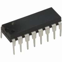
... Devices also available in Tape and Reel. Specify by appending the suffix letter “X” to the ordering code. Connection Diagram Pin Assignments for DIP, SOIC, SOP and TSSOP Top View © 1999 Fairchild Semiconductor Corporation loading is inhibited as long as the SHIFT/LOAD input is HIGH. When taken LOW, data at the parallel inputs is loaded directly into the register independent of the state of the clock ...

Page 2

Logic Diagrams www.fairchildsemi.com 2 ...

Page 3

Absolute Maximum Ratings (Note 2) Supply Voltage ( Input Voltage ( Output Voltage (V ) OUT Clamp Diode Current ( Output Current, per pin (I ) OUT DC ...

Page 4

AC Electrical Characteristics Symbol Parameter f Maximum Operating Frequency MAX Maximum Propagation Delay PHL PLH t , ...

Page 5

AC Electrical Characteristics Symbol Parameter C Power Dissipation (per package) PD Capacitance (Note 5) C Maximum Input Capacitance IN Note 5: C determines the no load dynamic power consumption ...

Page 6

Physical Dimensions inches (millimeters) unless otherwise noted 16-Lead Small Outline Integrated Circuit (SOIC), JEDEC MS-012, 0.150” Narrow 16-Lead Small Outline Package (SOP), EIAJ TYPE II, 5.3mm Wide www.fairchildsemi.com Package Number M16A Package Number M16D 6 ...

Page 7

Physical Dimensions inches (millimeters) unless otherwise noted (Continued) 16-Lead Thin Shrink Small Outline Package (TSSOP), JEDEC MO-153, 4.4mm Wide Package Number MTC16 7 www.fairchildsemi.com ...

Page 8

Physical Dimensions inches (millimeters) unless otherwise noted (Continued) 16-Lead Plastic Dual-In-Line Package (PDIP), MS-001, 0.300” Wide LIFE SUPPORT POLICY FAIRCHILD’S PRODUCTS ARE NOT AUTHORIZED FOR USE AS CRITICAL COMPONENTS IN LIFE SUPPORT DEVICES OR SYSTEMS WITHOUT THE EXPRESS WRITTEN APPROVAL ...

Related keywords