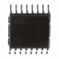
STPIC6D595TTR STMicroelectronics, STPIC6D595TTR Datasheet

STPIC6D595TTR
Specifications of STPIC6D595TTR
Available stocks
Related parts for STPIC6D595TTR
STPIC6D595TTR Summary of contents
Page 1
... Table 1. Device summary Order codes STPIC6D595MTR STPIC6D595TTR STPIC6D595B1R November 2009 Power logic 8-bit shift register SO-16 When data in the output buffers is low, the DMOS transistor outputs are off. When data is high, the DMOS transistor outputs have sink-current capability ...
Page 2
Contents Contents 1 Logic symbol and pin configuration . . . . . . . . . . . . . . . . . . . . . . . . . . . . 3 2 Maximum rating ...
Page 3
STPIC6D595 1 Logic symbol and pin configuration Figure 1. Pin configuration Figure 2. Logic symbol Logic symbol and pin configuration Doc ID 13663 Rev 3 3/21 ...
Page 4
Maximum rating 2 Maximum rating Stressing the device above the rating listed in the “absolute maximum ratings” table may cause permanent damage to the device. These are stress ratings only and operation of the device at these or any other ...
Page 5
STPIC6D595 2.3 Recommended operating conditions Table 4. Recommended operating conditions Symbol V Logic supply voltage CC V High level input voltage IH V Low level input voltage IL Pulse drain output current ° ...
Page 6
Electrical characteristics 3 Electrical characteristics 3.1 DC characteristics °C, unless otherwise specified Table 5. DC characteristics Symbol Parameter Drain-to-source V (BR)DSX breakdown voltage Source-to-drain diode V SD forward voltage High level ...
Page 7
STPIC6D595 3.2 Switching characteristics °C, unless otherwise specified Table 6. Switching characteristics Symbol Propagation delay time, high t PHL to low level output from G Propagation delay time, low t PLH ...
Page 8
Logic diagram 4 Logic diagram Figure 3. Logic diagram 8/21 Doc ID 13663 Rev 3 STPIC6D595 ...
Page 9
STPIC6D595 5 Typical operating circuit Figure 4. Typical operation mode test circuits Figure 5. Typical operation mode waveforms Note The word generator has the following characteristics: t pulse repetition rate (PRR kHz ...
Page 10
Typical operating circuit Figure 6. Typical operation mode test circuits Figure 7. Switching time waveform 10/21 Doc ID 13663 Rev 3 STPIC6D595 ...
Page 11
STPIC6D595 Figure 8. Input setup and hold waveform SRCK Note The word generator has the following characteristics: t pulse repetition rate (PRR kHz includes probe and jig capacitance ...
Page 12
Typical operating circuit Figure 9. Input equivalent circuit Figure 10. Output equivalent circuit 12/21 Doc ID 13663 Rev 3 STPIC6D595 ...
Page 13
STPIC6D595 6 Typical performance and characteristics Unless otherwise specified T Figure 11. Static drain-source on-state resistance vs logic supply voltage 5 R (Ω) DSon = 125 ° 4 ° 3 °C ...
Page 14
Package mechanical data 7 Package mechanical data In order to meet environmental requirements, ST offers these devices in different grades of ® ECOPACK packages, depending on their level of environmental compliance. ECOPACK specifications, grade definitions and product status are available ...
Page 15
STPIC6D595 DIM Plastic DIP-16 (0.25) MECHANICAL DATA mm. MIN. TYP MAX. 0.51 0.77 1.65 0.5 0.25 20 8.5 2.54 17.78 7.1 5.1 3.3 1.27 Doc ID 13663 Rev ...
Page 16
Package mechanical data DIM 16/21 SO-16 MECHANICAL DATA mm. MIN. TYP MAX. 1.75 0.1 0.25 1.64 0.35 0.46 0.19 0.25 0.5 9.8 10 5.8 ...
Page 17
STPIC6D595 DIM Tape & Reel SO-16 MECHANICAL DATA mm. MIN. TYP MAX. 330 12.8 13.2 20.2 60 22.4 6.45 6.65 10.3 10.5 2.1 2.3 3.9 4.1 7.9 8.1 Doc ID ...
Page 18
Package mechanical data DIM PIN 1 IDENTIFICATION 18/21 TSSOP16 MECHANICAL DATA mm. MIN. TYP MAX. 1.2 0.05 0.15 0.8 1 1.05 0.19 0.30 0.09 0.20 4.9 5 ...
Page 19
STPIC6D595 DIM Tape & Reel TSSOP16 MECHANICAL DATA mm. MIN. TYP MAX. 330 12.8 13.2 20.2 60 22.4 6.7 6.9 5.3 5.5 1.6 1.8 3.9 4.1 7.9 8.1 Doc ID ...
Page 20
Revision history 8 Revision history Table 7. Document revision history Date 20-Jun-2007 06-Sep-2007 17-Nov-2009 20/21 Revision 1 First release 2 Change from Preliminary to final version Updated: Table 2, Table Figure 7, Figure 8 and 3 Added: Figure 2, Figure ...
Page 21
... STPIC6D595 Information in this document is provided solely in connection with ST products. STMicroelectronics NV and its subsidiaries (“ST”) reserve the right to make changes, corrections, modifications or improvements, to this document, and the products and services described herein at any time, without notice. All ST products are sold pursuant to ST’s terms and conditions of sale. ...


