HCF4066M013TR STMicroelectronics, HCF4066M013TR Datasheet
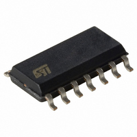
IC BILATERAL SWITCH QUAD 14-SOIC

HCF4066M013TR

Manufacturer Part Number
HCF4066M013TR
Description
IC BILATERAL SWITCH QUAD 14-SOIC
Manufacturer
STMicroelectronics
Series
4000r
Type
Bilateral, FET Switchesr
Datasheet

Specifications of HCF4066M013TR

Circuit
1 x 1:1
Independent Circuits
4
Voltage Supply Source
Dual Supply
Voltage - Supply
3 V ~ 20 V
Operating Temperature
-55°C ~ 125°C
Mounting Type
Surface Mount
Package / Case
14-SOIC (3.9mm Width), 14-SOL
Package
14SOP
Maximum On Resistance
1050@5V Ohm
Maximum Propagation Delay Bus To Bus
40 ns
Maximum Turn-on Time
70@5V ns
Switch Architecture
SPST
Power Supply Type
Single
Lead Free Status / RoHS Status
Lead free / RoHS Compliant
Current - Output High, Low
-
Other names
497-1134-2

Available stocks

Company
Part Number
Manufacturer
Quantity
Price
Part Number:
HCF4066M013TR
Manufacturer:
RENESAS
Quantity:
6 700
Part Number:
HCF4066M013TR
Manufacturer:
ST
0
Part Number:
HCF4066M013TR
Manufacturer:
ST
Quantity:
20 000
Part Number:
HCF4066M013TR
Manufacturer:
ST
Quantity:
17 374
Part Number:
HCF4066M013TR
Manufacturer:
ST
Quantity:
19 180
PIN CONNECTION
March 2004
15V DIGITAL OR ± 7.5V PEAK TO PEAK
SWITCHING
125 TYPICAL ON RESISTANCE FOR 15V
OPERATION
SWITCH ON RESISTANCE MATCHED TO
WITHIN 5
RANGE
ON RESISTANCE FLAT OVER FULL PEAK
TO PEAK SIGNAL RANGE
HIGH ON/OFF OUTPUT VOLTAGE RATIO:
65dB TYP. at f
HIGH DEGREE OF LINEARITY: < 0.5%
DISTORTION TYP. at f
V
EXTREMELY LOW OFF SWITCH LEAKAGE
RESULTING IN VERY LOW OFFSET
CURRENT AND HIGH EFFECTIVE OFF
RESISTANCE: 10pA TYP.
at V
EXTREMELY HIGH CONTROL INPUT
IMPEDANCE (control circuit isolated from
signal circuit 10
LOW CROSSTALK BETWEEN SWITCHES:
50dB Typ. at f
MATCHED CONTROL - INPUT TO SIGNAL
OUTPUT CAPACITANCE: REDUCES
OUTPUT SIGNAL TRANSIENTS
FREQUENCY RESPONSE SWITCH ON:
40MHz (Typ.)
QUIESCENT CURRENT SPECIF. UP TO 20V
5V, 10V AND 15V PARAMETRIC RATINGS
DD
DD
- V
- V
SS
QUAD BILATERAL SWITCH FOR TRANSMISSION OR
SS
> 10V, RL = 10K
TYP. OVER 15V SIGNAL INPUT
MULTIPLEXING OF ANALOG OR DIGITAL SIGNALS
= 10V, T
IS
IS
12
= 0.9MHz, R
= 10KHz, R
typ.)
amb
IS
= 1KHz, V
= 25°C
L
L
= 10K
= 1K
IS
= 5 V
pp
,
ORDER CODES
DESCRIPTION
The HCF4066B is a monolithic integrated circuit
fabricated
technology available in DIP and SOP packages.
The HCF4066B is a QUAD BILATERAL SWITCH
intended for the transmission or multiplexing of
analog or digital signals.
It is pin for pin compatible with HCF4016B, but
exhibits a much lower ON resistance. In addition,
the ON resistance is relatively constant over the
full input signal range. The HCF4066B consists of
four independent bilateral switches. A single
control signal is required per switch. Both the p
PACKAGE
INPUT LEAKAGE CURRENT
I
100% TESTED FOR QUIESCENT CURRENT
SOP
I
DIP
= 100nA (MAX) AT V
in
DIP
HCF4066BM1
HCF4066BEY
Metal
TUBE
Oxide
DD
HCF4066B
= 18V T
HCF4066M013TR
SOP
Semiconductor
A
T & R
= 25°C
1/10

Related parts for HCF4066M013TR

HCF4066M013TR Summary of contents

Page 1

... ON resistance. In addition, the ON resistance is relatively constant over the full input signal range. The HCF4066B consists of four independent bilateral switches. A single control signal is required per switch. Both the p HCF4066B DIP SOP TUBE T & R HCF4066BEY HCF4066BM1 HCF4066M013TR = 18V T = 25° Metal Oxide Semiconductor 1/10 ...

Page 2

HCF4066B and n device in a given switch are biased ON or OFF simultaneously by the control signal. As shown in schematic diagram, the well of the n-channel device on each switch is either tied to the input when the ...

Page 3

ABSOLUTE MAXIMUM RATINGS Symbol V Supply Voltage Input Voltage Input Current I P Power Dissipation per Package D Power Dissipation per Output Transistor T Operating Temperature op T Storage Temperature stg Absolute Maximum Ratings ...

Page 4

HCF4066B Symbol Parameter -50dB Crosstalk Frequency t Propagation Delay pd Time (signal input to output) square wave centered Input Capacitance IS Output C OS Capacitance C Feedthrough IOS Input/Output Leakage Current V IS Switch OFF V IS ...

Page 5

TYPICAL APPLICATIONS (BIDIRECTIONAL SIGNAL TRANSMISSION VIA DIGITAL CONTROL LOGIC) TYPICAL APPLICATIONS (4-CHANNEL PAM MULTIPLEXER SYSTEM DIAGRAM) HCF4066B 5/10 ...

Page 6

HCF4066B TEST CIRCUIT C = 50pF or equivalent (includes jig and probe capacitance 200K pulse generator (typically OUT WAVEFORM: PROPAGATION DELAY TIMES (f=1MHz; 50% duty cycle) 6/10 ...

Page 7

Plastic DIP-14 MECHANICAL DATA mm. DIM. MIN. a1 0. 15. 1.27 TYP MAX. MIN. 0.020 1.65 0.055 0.5 0.25 20 8.5 2.54 7.1 5.1 3.3 2.54 0.050 HCF4066B ...

Page 8

HCF4066B DIM. MIN 0 0. 8. 3.8 G 4 8/10 SO-14 MECHANICAL DATA mm. TYP MAX. 1.75 0.2 1.65 0.46 0.25 0.5 ...

Page 9

Tape & Reel SO-14 MECHANICAL DATA mm. DIM. MIN 12 2.1 Po 3.9 P 7.9 TYP MAX. MIN. 330 13.2 0.504 0.795 2.362 22.4 6.6 0.252 9.2 0.354 ...

Page 10

... No license is granted by implication or otherwise under any patent or patent rights of STMicroelectronics. Specifications mentioned in this publication are subject to change without notice. This publication supersedes and replaces all information previously supplied ...

Related keywords