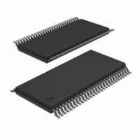
CBT6832DDGG,118 NXP Semiconductors, CBT6832DDGG,118 Datasheet - Page 5

CBT6832DDGG,118
Manufacturer Part Number
CBT6832DDGG,118
Description
IC 16BIT 1OF2 MUX/DEMUX 56TSSOP
Manufacturer
NXP Semiconductors
Series
74CBTr
Type
Multiplexer/Demultiplexerr
Datasheet
1.CBT6832DDGG112.pdf
(8 pages)
Specifications of CBT6832DDGG,118
Circuit
16 x 1:2
Independent Circuits
1
Current - Output High, Low
15mA, 64mA
Voltage Supply Source
Single Supply
Voltage - Supply
4.5 V ~ 5.5 V
Operating Temperature
0°C ~ 70°C
Mounting Type
Surface Mount
Package / Case
56-TSSOP
Lead Free Status / RoHS Status
Lead free / RoHS Compliant
Other names
935267061118
CBT6832DDG-T
CBT6832DDG-T
CBT6832DDG-T
CBT6832DDG-T
1. This parameter is warranted but not production tested. The propagation delay is based on the RC time constant of the typical on-state
Philips Semiconductors
AC CHARACTERISTICS
V
NOTE:
AC WAVEFORMS
V
2000 Sep 01
CC
M
SYMBOL
SYMBOL
16-bit controlled enable rate 1-of-2 multiplexer/demultiplexer with precharged
outputs and charge pump undershoot protection for live insertion
OUTPUT
Waveform 1. Input (An) to Output (Bn) Propagation Delays
resistance of the switch and a load capacitance of 50 pF, when driven by an ideal voltage source (zero output impedance).
= 1.5 V, V
INPUT
Output Control
t
t
t
t
t
t
= 5.0 V 0.5 V; GND = 0 V
PLH
PHL
PZH
PHZ
PZL
PLZ
Waveform 2. 3-State Output Enable and Disable Times
Waveform 1
Waveform 2
S1 at Open
(see Note)
(see Note)
(Low-level
S1 at 7 V
enabling
Output
Output
IN
Note:
Waveform 1 is for an output with internal conditions such that
the output is low except when disabled by the output control.
Waveform 2 is for an output with internal conditions such that
the output is high except when disabled by the output control.
Propagation delay
A to B
Bus enable time
SEL to A, B
Bus disable time
SEL to A, B
t
PZH
t
= GND to 3.0 V
PZL
1.5V
t
PLH
1.5 V
1.5V
1.5 V
1.2 V
PARAMETER
PARAMETER
;
C
1
L
= 50 pF, R
t
PHZ
t
PLZ
1.5V
t
L
PHL
1.5 V
= 500
V
V
OL
OH
1.5V
SA00543
+ 0.3V
– 0.3V
SA00028
3V
0V
3 V
0 V
V
V
3.5V
V
V
0V
OH
OL
OL
OH
TEST CONDITIONS
TEST CONDITIONS
5
TEST CIRCUIT AND WAVEFORMS
DEFINITIONS
C
From Output
Under Test
L
=
C
Load capacitance includes jig and probe capacitance;
see AC CHARACTERISTICS for value.
L
= 50 pF
MIN
0.5
0.5
10
5
t
t
PHZ
PLZ
TEST
t
pd
/t
/t
PZL
PZH
500
Load Circuit
LIMITS
500
TYP
0.25
open
open
7 V
S1
S1
CBT6832D
Product specification
MAX
30
25
7 V
GND
SA00012
6
7
Open
UNIT
UNIT
ns
ns
ns


