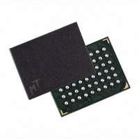
MT45W1MW16BDGB-708 AT TR Micron Technology Inc, MT45W1MW16BDGB-708 AT TR Datasheet - Page 25

MT45W1MW16BDGB-708 AT TR
Manufacturer Part Number
MT45W1MW16BDGB-708 AT TR
Description
IC PSRAM 16MBIT 70NS 54VFBGA
Manufacturer
Micron Technology Inc
Datasheet
1.MT45W1MW16BDGB-708_AT_TR.pdf
(59 pages)
Specifications of MT45W1MW16BDGB-708 AT TR
Format - Memory
RAM
Memory Type
PSRAM (Page)
Memory Size
16M (1M x 16)
Speed
70ns
Interface
Parallel
Voltage - Supply
1.7 V ~ 1.95 V
Operating Temperature
-30°C ~ 85°C
Package / Case
54-VFBGA
Lead Free Status / RoHS Status
Lead free / RoHS Compliant
Other names
557-1419-2
Output Impedance (BCR[5]) Default = Outputs Use Full Drive Strength
WAIT Configuration (BCR[8]) Default = WAIT Transitions One Clock Before Data Valid/Invalid
WAIT Polarity (BCR[10]) Default = WAIT Active HIGH
Figure 18:
Figure 19:
PDF: 09005aef81cb58ed/Source: 09005aef81c7a667
16mb_burst_cr1_0_p23z_2.fm - Rev. H 4/08 EN
WAIT Configuration (BCR[8] = 0)
WAIT Configuration (BCR[8] = 1)
Note:
Note:
The output driver strength can be altered to adjust for different data bus loading
scenarios. The reduced-strength option should be more than adequate in stacked chip
(Flash + CellularRAM) environments when there is a dedicated memory bus. The reduced-
drive-strength option is included to minimize noise generated on the data bus during
READ operations. Normal output impedance should be selected when using a discrete
CellularRAM device in a more heavily loaded data bus environment. Partial drive is
approximately one-quarter full drive strength. Outputs are configured at full drive
strength during testing.
The WAIT configuration bit is used to determine when WAIT transitions between the
asserted and the de-asserted state with respect to valid data presented on the data bus.
The memory controller will use the WAIT signal to coordinate data transfer during
synchronous READ and WRITE operations. When BCR[8] = 0, data will be valid or invalid
on the clock edge immediately after WAIT transitions to the de-asserted or asserted
state, respectively (see Figures 18 and 20). When BCR[8] = 1, the WAIT signal transitions
one clock period prior to the data bus going valid or invalid (see Figures 19 and 20).
The WAIT polarity bit indicates whether an asserted WAIT output should be HIGH or
LOW. This bit will determine whether the WAIT signal requires a pull-up or pull-down
resistor to maintain the de-asserted state.
DQ[15:0]
D[15:0]
WAIT
CLK
WAIT
Data valid/invalid immediately after WAIT transitions (BCR[8] = 0). See Figure 20 on
page 26.
Valid/invalid data delayed for one clock after WAIT transitions (BCR[8] = 1). See Figure 20
on page 26.
CLK
Data valid (or invalid) after one clock delay
16Mb: 1 Meg x 16 Async/Page/Burst CellularRAM 1.0 Memory
High-Z
Data immediately valid (or invalid)
High-Z
Data[0]
Data[0]
Data[1]
25
Micron Technology, Inc., reserves the right to change products or specifications without notice.
Configuration Registers
©2005 Micron Technology, Inc. All rights reserved.


