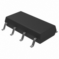
S-24CS01AFJ-TB-G Seiko Instruments, S-24CS01AFJ-TB-G Datasheet - Page 16

S-24CS01AFJ-TB-G
Manufacturer Part Number
S-24CS01AFJ-TB-G
Description
IC EEPROM 1KBIT 400KHZ 8SOP
Manufacturer
Seiko Instruments
Datasheet
1.S-24CS01AFT-TB-G.pdf
(47 pages)
Specifications of S-24CS01AFJ-TB-G
Format - Memory
EEPROMs - Serial
Memory Type
EEPROM
Memory Size
1K (128 x 8)
Speed
400kHz
Interface
I²C, 2-Wire Serial
Voltage - Supply
1.8 V ~ 5.5 V
Operating Temperature
-40°C ~ 85°C
Package / Case
8-SOP
Lead Free Status / RoHS Status
Lead free / RoHS Compliant
Available stocks
Company
Part Number
Manufacturer
Quantity
Price
Company:
Part Number:
S-24CS01AFJ-TB-G
Manufacturer:
SEIKO
Quantity:
576
16
2-WIRE CMOS SERIAL E
S-24CS01A/02A/04A/08A
7. Read
7. 1 Current Address Read
Either in writing or in reading the E
incremented by one. The memory address is maintained as long as the power voltage is higher than the
current address hold voltage V
The master device can read the data at the memory address of the current address pointer without
assigning the word address as a result, when it recognizes the position of the address pointer in the
E
In the following the address counter in the E
When the E
following a start condition, it responds with an acknowledge. However, the page address (P0) in S-
24CS04A and the page address (P1 and P0) in S-24CS08A become invalid and the memory address of
the current address pointer becomes valid.
Next an 8-bit data at the address "n" is sent from the E
address counter is incremented at the falling edge of the SCL clock for the 8th bit data, and the content of
the address counter becomes n + 1.
The master device outputs stop condition not an acknowledge ,the reading of E
Attention should be paid to the following point on the recognition of the address pointer in the E
In the read operation the memory address counter in the E
falling edge of the SCL clock for the 8th bit of the output data. In the write operation, on the other hand,
the upper bits of the memory address (the upper bits of the word address and page address)
unchanged and are not incremented at the falling edge of the SCL clock for the 8th bit of the received
data.
*1. S-24CS01A/02A is the upper 5 bits of the word address.
2
PROM. This is called "Current Address Read".
S-24CS04A is the upper 4 bits of the word address and the page address P0.
S-24CS08A is the upper 4 bits of the word address and the page address P1 and P0.
2
PROM receives a 7-bit device address and a 1-bit read / write instruction code set to “1”
SDA LINE
Remark1. A1 is P1 in S-24CS08A.
2
PROM
2. A0 is P0 in S-24CS04A/08A.
S
T
A
R
T
AH
.
M
S
B
1 0 1 0
Figure 16 Current Address Read
Seiko Instruments Inc.
ADDRESS
DEVICE
2
PROM holds the last accessed memory address, internally
A2 A1 A0
2
PROM is assumed to be “n”.
L
S
B
W
R
R
E
A
D
1
/
A
C
K
D7 D6 D5 D4 D3 D2 D1 D0
2
2
PROM is automatically incremented at every
PROM synchronous to the SCL clock. The
NO ACK from
Master Device
DATA
ADR INC
2
PROM is ended.
S
T
O
P
Rev.4.5
2
PROM.
*1
are left
_00


