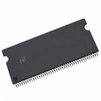
MT48LC2M32B2P-55:G Micron Technology Inc, MT48LC2M32B2P-55:G Datasheet - Page 20

MT48LC2M32B2P-55:G
Manufacturer Part Number
MT48LC2M32B2P-55:G
Description
IC SDRAM 64MBIT 5.5NS 86TSOP
Manufacturer
Micron Technology Inc
Datasheet
1.MT48LC2M32B2P-6G_TR.pdf
(69 pages)
Specifications of MT48LC2M32B2P-55:G
Format - Memory
RAM
Memory Type
SDRAM
Memory Size
64M (2Mx32)
Speed
5.5ns
Interface
Parallel
Voltage - Supply
3 V ~ 3.6 V
Operating Temperature
0°C ~ 70°C
Package / Case
86-TSOP
Lead Free Status / RoHS Status
Lead free / RoHS Compliant
Figure 6:
Figure 7:
READs
PDF: 09005aef811ce1fe/Source: 09005aef811ce1d5
64MSDRAMx32_2.fm - Rev. J 12/08 EN
Activating a Specific Row in a Specific Bank
Example: Meeting
Notes:
COMMAND
1.
2.
READ bursts are initiated with a READ command, as shown in Figure 8 on page 21.
The starting column and bank addresses are provided with the READ command, and
auto precharge either is enabled or disabled for that burst access. If auto precharge is
enabled, the row being accessed is precharged at the completion of the burst. For the
generic READ commands used in the following illustrations, auto precharge is disabled.
During READ bursts, the valid data-out element from the starting column address will
be available following the CAS latency after the READ command. Each subsequent data-
out element will be valid by the next positive clock edge. Figure 9 on page 22 shows
general timing for each possible CAS latency setting.
BA0, BA1
A0–A10
t
t
RAS#
CAS#
RCD (MIN) = 20ns,
RCD (MIN) x
WE#
CKE
CLK
CLK
CS#
t
RCD (MIN) when 2 <
HIGH
ACTIVE
T0
t
CK where x = number of clocks for equation to be true.
t CK
t
CK = 8ns.
t
t RCD (MIN) +0.5 t CK
NOP
RCD (MIN)
ADDRESS
ADDRESS
T1
BANK
ROW
20
t CK
t
DON´T CARE
RCD (MIN)/
NOP
Micron Technology, Inc., reserves the right to change products or specifications without notice.
T2
t CK
t
CK - 3
READ or
DON’T CARE
WRITE
T3
©2001 Micron Technology, Inc. All rights reserved.
64Mb: x32 SDRAM
Commands


