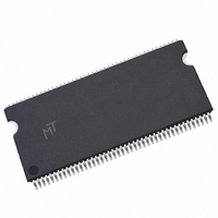
MT48LC2M32B2P-5:G Micron Technology Inc, MT48LC2M32B2P-5:G Datasheet - Page 49

MT48LC2M32B2P-5:G
Manufacturer Part Number
MT48LC2M32B2P-5:G
Description
IC SDRAM 64MBIT 200MHZ 86TSOP
Manufacturer
Micron Technology Inc
Type
SDRAMr
Datasheet
1.MT48LC2M32B2P-6G_TR.pdf
(69 pages)
Specifications of MT48LC2M32B2P-5:G
Format - Memory
RAM
Memory Type
SDRAM
Memory Size
64M (2Mx32)
Speed
200MHz
Interface
Parallel
Voltage - Supply
3 V ~ 3.6 V
Operating Temperature
0°C ~ 70°C
Package / Case
86-TSOP
Organization
2Mx32
Density
64Mb
Address Bus
13b
Access Time (max)
4.5ns
Maximum Clock Rate
200MHz
Operating Supply Voltage (typ)
3.3V
Package Type
TSOP-II
Operating Temp Range
0C to 70C
Operating Supply Voltage (max)
3.6V
Operating Supply Voltage (min)
3V
Supply Current
280mA
Pin Count
86
Mounting
Surface Mount
Operating Temperature Classification
Commercial
Package
86TSOP-II
Address Bus Width
13 Bit
Operating Supply Voltage
3.3 V
Maximum Random Access Time
4.5 ns
Lead Free Status / RoHS Status
Lead free / RoHS Compliant
Notes
PDF: 09005aef811ce1fe/Source: 09005aef811ce1d5
64MSDRAMx32_2.fm - Rev. J 12/08 EN
10.
11. AC timing and I
12. Other input signals are allowed to transition no more than once in any two-clock
13. I
14. Timing is actually specified by
15. Timing is actually specified by
16. Timing actually specified by
17. Required clocks are specified by JEDEC functionality and are not dependent on any
18. The I
19. Address transitions average one transition every two clocks.
20. CLK must be toggled a minimum of two times during this period.
21. Based on
22. V
1. All voltages referenced to V
2. This parameter is sampled. V
3. I
4. Enables on-chip refresh and address counters.
5. The minimum specifications are used only to indicate cycle time at which proper
6. An initial pause of 100µs is required after power-up, followed by two AUTO REFRESH
7. AC characteristics assume
8. In addition to meeting the transition rate specification, the clock and CKE must tran-
9. Outputs measured at 1.5V with equivalent load:
biased at 1.4V. AC can range from 0pF to 6pF.
with minimum cycle time and the outputs open.
operation over the full temperature range (0°C ≤ T
+85°C (industrial), and
commands, before proper device operation is ensured (V
ered up simultaneously. V
REFRESH command wake-ups should be repeated any time the
ment is exceeded.
sit between V
Q
t
a reference to V
High-Z.
crossover point.
period and are otherwise at valid V
mum cycle rate.
only at minimum cycle rate.
timing parameter.
imum cycle rate is slower as the CL is reduced.
cannot be greater than one-third the cycle rate. V
pulse width ≤ 3ns, and the pulse width cannot be greater than one-third the cycle rate.
DD
HZ defines the time at which the output achieves the open circuit condition; it is not
DD
IH
is dependent on output loading and cycle rates. Specified values are obtained
specifications are tested after the device is properly initialized.
overshoot: V
DD
current will decrease as the CL is reduced. This is due to the fact that the max-
t
CK = 143 MHz for -7, 166 MHz for -6, 183 MHz for -55, and 200 MHz for -5.
IH
30pF
OH
DD
and V
IH
(MAX) = V
or V
tests have V
IL
OL
–
(or between V
40°C ≤ T
. The last valid data element will meet
SS
t
49
SS
T = 1ns.
and V
t
DD
.
DD
WR.
IL
t
t
CKS; clock(s) specified as a reference only at mini-
WR plus
Q + 1.2V for a pulse width ≤ 3ns, and the pulse width
, V
A
= 0.25 and V
≤ +105°C (automotive) is ensured.
SS
DD
IH
Q must be at same potential). The two AUTO
Micron Technology, Inc., reserves the right to change products or specifications without notice.
Q = +3.3V; f = 1 MHz, T
or V
IL
and V
t
RP; clock(s) is (are) specified as a reference
IL
levels.
IH
IH
= 2.75, with timing referenced to 1.5V
) in a monotonic manner.
IL
A
≤ +70°C (commercial),
undershoot: V
DD
©2001 Micron Technology, Inc. All rights reserved.
A
and V
= 25°C; pin under test
64Mb: x32 SDRAM
t
OH before going
t
REF refresh require-
IL
DD
(MIN) = -1.2V for a
Q must be pow-
–
40°C ≤ T
Notes
A
≤


