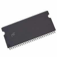
MT48LC8M16A2P-75:G Micron Technology Inc, MT48LC8M16A2P-75:G Datasheet - Page 28

MT48LC8M16A2P-75:G
Manufacturer Part Number
MT48LC8M16A2P-75:G
Description
IC SDRAM 128MBIT 133MHZ 54TSOP
Manufacturer
Micron Technology Inc
Type
SDRAMr
Specifications of MT48LC8M16A2P-75:G
Memory Type
SDRAM
Format - Memory
RAM
Memory Size
128M (8Mx16)
Speed
133MHz
Interface
Parallel
Voltage - Supply
3 V ~ 3.6 V
Operating Temperature
0°C ~ 70°C
Package / Case
54-TSOP II
Memory Configuration
16M X 8
Access Time
5.4ns
Page Size
128Mbit
Memory Case Style
TSOP
No. Of Pins
54
Operating Temperature Range
0°C To +70°C
Organization
8Mx16
Density
128Mb
Address Bus
14b
Access Time (max)
6/5.4ns
Maximum Clock Rate
133MHz
Operating Supply Voltage (typ)
3.3V
Package Type
TSOP-II
Operating Temp Range
0C to 70C
Operating Supply Voltage (max)
3.6V
Operating Supply Voltage (min)
3V
Supply Current
150mA
Pin Count
54
Mounting
Surface Mount
Operating Temperature Classification
Commercial
Lead Free Status / RoHS Status
Lead free / RoHS Compliant
Lead Free Status / RoHS Status
Compliant, Lead free / RoHS Compliant
Available stocks
Company
Part Number
Manufacturer
Quantity
Price
Company:
Part Number:
MT48LC8M16A2P-75:G
Manufacturer:
MICRON
Quantity:
8
Part Number:
MT48LC8M16A2P-75:G
Manufacturer:
MICRON
Quantity:
20 000
Figure 14:
PDF: 09005aef8091e66d/Source: 09005aef8091e625
128MSDRAM_2.fm - Rev. N 1/09 EN
Random READ Accesses
Notes:
COMMAND
COMMAND
1. Each READ command may be to any bank. DQM is LOW.
Data from any READ burst may be truncated with a subsequent WRITE command, and
data from a fixed-length READ burst may be immediately followed by data from a
WRITE command (subject to bus turnaround limitations). The WRITE burst may be
initiated on the clock edge immediately following the last (or last desired) data element
from the READ burst, provided that I/O contention can be avoided. In a given system
design, there may be a possibility that the device driving the input data will go Low-Z
before the SDRAM DQ go High-Z. In this case, at least a single-cycle delay should occur
between the last read data and the WRITE command.
The DQM input is used to avoid I/O contention, as shown in Figure 15 on page 29 and
Figure 16 on page 29. The DQM signal must be asserted (HIGH) at least 2 clocks prior to
the WRITE command (DQM latency is 2 clocks for output buffers) to suppress data-out
from the READ. After the WRITE command is registered, the DQ will go High-Z (or
remain High-Z), regardless of the state of the DQM signal, provided the DQM was active
on the clock just prior to the WRITE command that truncated the READ command. If
not, the second WRITE will be an invalid WRITE. For example, if DQM was LOW during
T4 in Figure 16, then the WRITEs at T5 and T7 would be valid, while the WRITE at T6
would be invalid.
ADDRESS
ADDRESS
CLK
CLK
DQ
DQ
T0
BANK,
T0
COL n
BANK,
COL n
READ
READ
CL = 2
T1
T1
BANK,
BANK,
READ
COL a
READ
COL a
CL = 3
28
T2
BANK,
T2
COL x
BANK,
READ
READ
COL x
D
OUT
n
TRANSITIONING DATA
Micron Technology, Inc., reserves the right to change products or specifications without notice.
T3
T3
BANK,
COL m
READ
READ
BANK,
COL m
D
D
OUT
a
OUT
n
T4
T4
NOP
NOP
D
D
OUT
x
OUT
a
128Mb: x4, x8, x16 SDRAM
T5
T5
NOP
NOP
D
D
m
OUT
OUT
x
©1999 Micron Technology, Inc. All rights reserved.
DON’T CARE
T6
NOP
D
OUT
m
Operations


