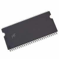
MT48LC8M16A2P-75:G Micron Technology Inc, MT48LC8M16A2P-75:G Datasheet - Page 36

MT48LC8M16A2P-75:G
Manufacturer Part Number
MT48LC8M16A2P-75:G
Description
IC SDRAM 128MBIT 133MHZ 54TSOP
Manufacturer
Micron Technology Inc
Type
SDRAMr
Specifications of MT48LC8M16A2P-75:G
Memory Type
SDRAM
Format - Memory
RAM
Memory Size
128M (8Mx16)
Speed
133MHz
Interface
Parallel
Voltage - Supply
3 V ~ 3.6 V
Operating Temperature
0°C ~ 70°C
Package / Case
54-TSOP II
Memory Configuration
16M X 8
Access Time
5.4ns
Page Size
128Mbit
Memory Case Style
TSOP
No. Of Pins
54
Operating Temperature Range
0°C To +70°C
Organization
8Mx16
Density
128Mb
Address Bus
14b
Access Time (max)
6/5.4ns
Maximum Clock Rate
133MHz
Operating Supply Voltage (typ)
3.3V
Package Type
TSOP-II
Operating Temp Range
0C to 70C
Operating Supply Voltage (max)
3.6V
Operating Supply Voltage (min)
3V
Supply Current
150mA
Pin Count
54
Mounting
Surface Mount
Operating Temperature Classification
Commercial
Lead Free Status / RoHS Status
Lead free / RoHS Compliant
Lead Free Status / RoHS Status
Compliant, Lead free / RoHS Compliant
Available stocks
Company
Part Number
Manufacturer
Quantity
Price
Company:
Part Number:
MT48LC8M16A2P-75:G
Manufacturer:
MICRON
Quantity:
8
Part Number:
MT48LC8M16A2P-75:G
Manufacturer:
MICRON
Quantity:
20 000
PRECHARGE
Figure 26:
Power-Down
PDF: 09005aef8091e66d/Source: 09005aef8091e625
128MSDRAM_2.fm - Rev. N 1/09 EN
PRECHARGE Command
The PRECHARGE command (see Figure 26) is used to deactivate the open row in a
particular bank or the open row in all banks. The bank(s) will be available for a subse-
quent row access some specified time (
Input A10 determines whether one or all banks are to be precharged, and in the case
where only one bank is to be precharged, inputs BA0, BA1 select the bank. When all
banks are to be precharged, inputs BA0, BA1 are treated as “Don’t Care.” After a bank has
been precharged, it is in the idle state and must be activated prior to any READ or WRITE
commands being issued to that bank.
BA0, BA1
Power-down occurs if CKE is registered LOW coincident with a NOP or COMMAND
INHIBIT when no accesses are in progress. If power-down occurs when all banks are
idle, this mode is referred to as precharge power-down; if power-down occurs when
there is a row active in any bank, this mode is referred to as active power-down. Entering
power-down deactivates the input and output buffers, excluding CKE, for maximum
power savings while in standby. The device may not remain in the power-down state
longer than the refresh period (
performed in this mode.
The power-down state is exited by registering a NOP or COMMAND INHIBIT and CKE
HIGH at the desired clock edge (meeting
A0–A9
RAS#
CAS#
WE#
CKE
A10
CLK
CS#
HIGH
VALID ADDRESS
Bank Selected
All Banks
ADDRESS
BANK
36
t
REF or
DON’T CARE
Micron Technology, Inc., reserves the right to change products or specifications without notice.
t
t
RP) after the PRECHARGE command is issued.
REF
t
CKS). See Figure 27 on page 37.
AT
) since no REFRESH operations are
128Mb: x4, x8, x16 SDRAM
©1999 Micron Technology, Inc. All rights reserved.
Operations


