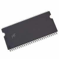
MT48LC8M16A2P-75:G Micron Technology Inc, MT48LC8M16A2P-75:G Datasheet - Page 52

MT48LC8M16A2P-75:G
Manufacturer Part Number
MT48LC8M16A2P-75:G
Description
IC SDRAM 128MBIT 133MHZ 54TSOP
Manufacturer
Micron Technology Inc
Type
SDRAMr
Specifications of MT48LC8M16A2P-75:G
Memory Type
SDRAM
Format - Memory
RAM
Memory Size
128M (8Mx16)
Speed
133MHz
Interface
Parallel
Voltage - Supply
3 V ~ 3.6 V
Operating Temperature
0°C ~ 70°C
Package / Case
54-TSOP II
Memory Configuration
16M X 8
Access Time
5.4ns
Page Size
128Mbit
Memory Case Style
TSOP
No. Of Pins
54
Operating Temperature Range
0°C To +70°C
Organization
8Mx16
Density
128Mb
Address Bus
14b
Access Time (max)
6/5.4ns
Maximum Clock Rate
133MHz
Operating Supply Voltage (typ)
3.3V
Package Type
TSOP-II
Operating Temp Range
0C to 70C
Operating Supply Voltage (max)
3.6V
Operating Supply Voltage (min)
3V
Supply Current
150mA
Pin Count
54
Mounting
Surface Mount
Operating Temperature Classification
Commercial
Lead Free Status / RoHS Status
Lead free / RoHS Compliant
Lead Free Status / RoHS Status
Compliant, Lead free / RoHS Compliant
Available stocks
Company
Part Number
Manufacturer
Quantity
Price
Company:
Part Number:
MT48LC8M16A2P-75:G
Manufacturer:
MICRON
Quantity:
8
Part Number:
MT48LC8M16A2P-75:G
Manufacturer:
MICRON
Quantity:
20 000
PDF: 09005aef8091e66d/Source: 09005aef8091e625
128MSDRAM_2.fm - Rev. N 1/09 EN
12. Other input signals are allowed to transition no more than once every 2 clocks and are
13. I
14. Timing actually specified by
15. Timing actually specified by
16. Timing actually specified by
17. Required clocks are specified by JEDEC functionality and are not dependent on any
18. The I
19. Address transitions average one transition every 2 clocks.
20. CLK must be toggled a minimum of two times during this period.
21. Based on
22. V
23. The clock frequency must remain constant (stable clock is defined as a signal cycling
24. Auto precharge mode only. The precharge timing budget (
25. Precharge mode only.
26. JEDEC and PC100 specify 3 clocks.
27.
28. Parameter guaranteed by design.
29. PC100 specifies a maximum of 4pF.
30. PC100 specifies a maximum of 5pF.
31. PC100 specifies a maximum of 6.5pF.
32. For -75, CL = 3 and
33. CKE is HIGH during refresh command period
34. PC133 specifies a minimum of 2.5pF.
35. PC133 specifies a minimum of 2.5pF.
36. PC133 specifies a minimum of 3.0pF.
otherwise at valid V
cycle rate.
minimum cycle rate.
timing parameter.
frequency alteration for the test condition.
cannot be greater than one-third of the cycle rate. V
a pulse width
within timing constraints specified for the clock pin) during access or precharge
states (READ, WRITE, including
used to reduce the data rate.
for -7E, and 7.5ns for -75 after the first clock delay, after the last WRITE is executed.
t
6ns.
limit is actually a nominal value and does not result in a fail value.
DD
AC for -75/-7E at CL = 3 with no load is 4.6ns and is guaranteed by design.
IH
specifications are tested after the device is properly initialized.
overshoot: V
DD
current will increase or decrease proportionally according to the amount of
t
CK = 7.5ns for -75/-7E, and
≤
3ns.
IH
(MAX) = V
t
IH
CK = 7.5ns; for -7E, CL = 2 and
or V
IL
52
levels.
t
t
t
CKS; clock(s) specified as a reference only at minimum
WR plus
WR.
DD
Q + 2V for a pulse width
t
WR, and PRECHARGE commands). CKE may be
Micron Technology, Inc., reserves the right to change products or specifications without notice.
t
t
CK = 6ns for -6A.
RP; clock(s) specified as a reference only at
t
RFC (MIN) else CKE is LOW. The I
t
128Mb: x4, x8, x16 SDRAM
CK = 7.5ns, and CL = 3 and
IL
undershoot: V
≤
3ns, and the pulse width
t
RP) begins 6ns for -6A, 7ns
©1999 Micron Technology, Inc. All rights reserved.
IL
(MIN) = –2V for
Notes
t
CK =
DD
6


