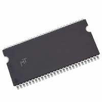
MT48LC32M8A2P-7E:D Micron Technology Inc, MT48LC32M8A2P-7E:D Datasheet - Page 35

MT48LC32M8A2P-7E:D
Manufacturer Part Number
MT48LC32M8A2P-7E:D
Description
IC SDRAM 256MBIT 133MHZ 54TSOP
Manufacturer
Micron Technology Inc
Type
SDRAMr
Datasheet
1.MT48LC16M16A2P-75D_TR.pdf
(92 pages)
Specifications of MT48LC32M8A2P-7E:D
Package / Case
54-TSOP II
Format - Memory
RAM
Memory Type
SDRAM
Memory Size
256M (32M x 8)
Speed
133MHz
Interface
Parallel
Voltage - Supply
3 V ~ 3.6 V
Operating Temperature
0°C ~ 70°C
Access Time
RoHS Compliant
Memory Case Style
TSOP
No. Of Pins
54
Operating Temperature Range
0°C To +70°C
Operating Temperature Max
70°C
Operating Temperature Min
0°C
Organization
32Mx8
Density
256Mb
Address Bus
15b
Access Time (max)
5.4ns
Maximum Clock Rate
143MHz
Operating Supply Voltage (typ)
3.3V
Package Type
TSOP-II
Operating Temp Range
0C to 70C
Operating Supply Voltage (max)
3.6V
Operating Supply Voltage (min)
3V
Supply Current
135mA
Pin Count
54
Mounting
Surface Mount
Operating Temperature Classification
Commercial
Memory Configuration
4 BLK (8M X 8)
Interface Type
LVTTL
Rohs Compliant
Yes
Lead Free Status / RoHS Status
Lead free / RoHS Compliant
WRITE
Figure 15: WRITE Command
PDF: 09005aef8091e6d1
256Mb_sdr.pdf - Rev. N 1/10 EN
Note:
The WRITE command is used to initiate a burst write access to an active row. The val-
ues on the BA0 and BA1 inputs select the bank; the address provided selects the starting
column location. The value on input A10 determines whether auto precharge is used. If
auto precharge is selected, the row being accessed is precharged at the end of the write
burst; if auto precharge is not selected, the row remains open for subsequent accesses.
Input data appearing on the DQ is written to the memory array, subject to the DQM
input logic level appearing coincident with the data. If a given DQM signal is registered
LOW, the corresponding data is written to memory; if the DQM signal is registered
HIGH, the corresponding data inputs are ignored and a WRITE is not executed to that
byte/column location.
BA0, BA1
Address
1. EN AP = enable auto precharge, DIS AP = disable auto precharge.
RAS#
CAS#
A10
WE#
CKE
CLK
CS#
1
HIGH
Valid address
Column address
Bank address
DIS AP
EN AP
35
Don’t Care
Micron Technology, Inc. reserves the right to change products or specifications without notice.
256Mb: x4, x8, x16 SDRAM
© 1999 Micron Technology, Inc. All rights reserved.
Commands


