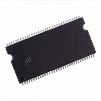
MT46V64M8P-6T:F Micron Technology Inc, MT46V64M8P-6T:F Datasheet - Page 23

MT46V64M8P-6T:F
Manufacturer Part Number
MT46V64M8P-6T:F
Description
IC DDR SDRAM 512MBIT 6NS 66TSOP
Manufacturer
Micron Technology Inc
Type
DDR SDRAMr
Datasheet
1.MT46V32M16P-5BF_TR.pdf
(91 pages)
Specifications of MT46V64M8P-6T:F
Format - Memory
RAM
Memory Type
DDR SDRAM
Memory Size
512M (64M x 8)
Speed
6ns
Interface
Parallel
Voltage - Supply
2.3 V ~ 2.7 V
Operating Temperature
0°C ~ 70°C
Package / Case
66-TSOP
Organization
64Mx8
Density
512Mb
Address Bus
15b
Access Time (max)
700ps
Maximum Clock Rate
333MHz
Operating Supply Voltage (typ)
2.5V
Package Type
TSOP
Operating Temp Range
0C to 70C
Operating Supply Voltage (max)
2.7V
Operating Supply Voltage (min)
2.3V
Supply Current
175mA
Pin Count
66
Mounting
Surface Mount
Operating Temperature Classification
Commercial
Lead Free Status / RoHS Status
Lead free / RoHS Compliant
Available stocks
Company
Part Number
Manufacturer
Quantity
Price
Company:
Part Number:
MT46V64M8P-6T:F
Manufacturer:
MICRON
Quantity:
6 538
Company:
Part Number:
MT46V64M8P-6T:F
Manufacturer:
IR
Quantity:
8 000
Part Number:
MT46V64M8P-6T:F
Manufacturer:
MICRON/美光
Quantity:
20 000
Table 18:
PDF: 09005aef80a1d9d4/Source: 09005aef82a95a3a
DDR_x4x8x16_Core2.fm - 512Mb DDR: Rev. N; Core DDR Rev. B 2/09 EN
AC Characteristics
Parameter
Access window of DQ from CK/CK#
CK high-level width
Clock cycle time
CK low-level width
DQ and DM input hold time relative to DQS
DQ and DM input pulse width (for each input)
Access window of DQS from CK/CK#
DQS input high pulse width
DQS input low pulse width
DQS–DQ skew, DQS to last DQ valid, per group, per access
WRITE command to first DQS latching transition
DQ and DM input setup time relative to DQS
DQS falling edge from CK rising – hold time
DQS falling edge to CK rising – setup time
Half-clock period
Data-out High-Z window from CK/CK#
Address and control input hold time (slew rate ≥0.5 V/ns)
Address and control input pulse width (for each input)
Address and control input setup time (slew rate ≥0.5 V/ns)
Data-out Low-Z window from CK/CK#
LOAD MODE REGISTER command cycle time
DQ–DQS hold, DQS to first DQ to go non-valid, per access
Data hold skew factor
ACTIVE-to-READ with auto precharge command
ACTIVE-to-PRECHARGE command
ACTIVE-to-ACTIVE/AUTO REFRESH command period
ACTIVE-to-READ or WRITE delay
REFRESH-to-REFRESH command interval
REFRESH-to-REFRESH command interval (Automotive)
Average periodic refresh interval
Average periodic refresh interval (Automotive)
AUTO REFRESH command period
PRECHARGE command period
DQS read preamble
DQS read postamble
ACTIVE bank a to ACTIVE bank b command
Terminating voltage delay to V
DQS write preamble
DQS write preamble setup time
DQS write postamble
Electrical Characteristics and Recommended AC Operating Conditions (-5B)
Notes 1–6, 16–18, 34 apply to the entire table; Notes appear on page 35;
0°C ≤ T
A
≤ +70°C; V
DD
DD
Q = +2.6V ±0.1V, V
CL = 3
CL = 2.5
CL = 2
DD
= +2.6V ±0.1V
23
t
Symbol
t
t
t
CK (2.5)
t
t
t
t
t
t
DQSCK
REFC
WPRES
t
t
t
t
t
t
t
REFI
t
CK (3)
CK (2)
DQSH
DQSQ
WPRE
DIPW
t
t
t
t
t
t
WPST
DQSL
DQSS
t
t
t
t
t
RPRE
MRD
REFC
RPST
t
t
t
t
DSH
t
t
t
QHS
RCD
REFI
RRD
VTD
t
IPW
t
RAP
RAS
t
t
t
DSS
t
RFC
DH
IH
QH
AC
CH
HP
HZ
DS
IS
RC
RP
CL
LZ
Micron Technology, Inc., reserves the right to change products or specifications without notice.
F
F
AT
AT
Electrical Specifications – DC and AC
t
HP -
t
CH,
512Mb: x4, x8, x16 DDR SDRAM
–0.70
–0.60
–0.70
Min
0.45
0.45
0.40
1.75
0.35
0.35
0.72
0.40
0.60
0.60
0.25
7.5
0.2
0.2
2.2
0.9
0.4
0.4
10
15
40
55
15
70
15
10
5
6
–
–
–
–
–
–
–
0
0
t
t
QHS
CL
-5B
70,000
+0.70
+0.60
+0.70
17.55
Max
0.55
0.55
0.40
1.28
0.50
70.3
1.95
7.5
7.8
1.1
0.6
0.6
13
13
–
–
–
–
–
–
–
–
–
–
–
–
–
–
–
–
–
–
–
–
–
–
–
©2000 Micron Technology, Inc. All rights reserved.
Units
t
t
t
t
t
t
t
t
t
t
t
ns
CK
ns
ns
ns
CK
ns
ns
ns
CK
CK
ns
CK
ns
CK
CK
ns
ns
ns
ns
ns
ns
ns
ns
ns
ns
ns
ns
ns
µs
µs
µs
µs
ns
ns
CK
CK
ns
ns
CK
ns
CK
Notes
46, 52
46, 52
27, 32
26, 27
27, 32
19, 43
19, 43
26, 27
21, 22
31
52
31
32
35
15
15
36
24
24
24
24
50
44
44
20


