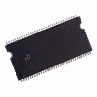
MT46V64M8P-6T:F Micron Technology Inc, MT46V64M8P-6T:F Datasheet - Page 35

MT46V64M8P-6T:F
Manufacturer Part Number
MT46V64M8P-6T:F
Description
IC DDR SDRAM 512MBIT 6NS 66TSOP
Manufacturer
Micron Technology Inc
Type
DDR SDRAMr
Datasheet
1.MT46V32M16P-5BF_TR.pdf
(91 pages)
Specifications of MT46V64M8P-6T:F
Format - Memory
RAM
Memory Type
DDR SDRAM
Memory Size
512M (64M x 8)
Speed
6ns
Interface
Parallel
Voltage - Supply
2.3 V ~ 2.7 V
Operating Temperature
0°C ~ 70°C
Package / Case
66-TSOP
Organization
64Mx8
Density
512Mb
Address Bus
15b
Access Time (max)
700ps
Maximum Clock Rate
333MHz
Operating Supply Voltage (typ)
2.5V
Package Type
TSOP
Operating Temp Range
0C to 70C
Operating Supply Voltage (max)
2.7V
Operating Supply Voltage (min)
2.3V
Supply Current
175mA
Pin Count
66
Mounting
Surface Mount
Operating Temperature Classification
Commercial
Lead Free Status / RoHS Status
Lead free / RoHS Compliant
Available stocks
Company
Part Number
Manufacturer
Quantity
Price
Company:
Part Number:
MT46V64M8P-6T:F
Manufacturer:
MICRON
Quantity:
6 538
Company:
Part Number:
MT46V64M8P-6T:F
Manufacturer:
IR
Quantity:
8 000
Part Number:
MT46V64M8P-6T:F
Manufacturer:
MICRON/美光
Quantity:
20 000
Notes
PDF: 09005aef80a1d9d4/Source: 09005aef82a95a3a
DDR_x4x8x16_Core2.fm - 512Mb DDR: Rev. N; Core DDR Rev. B 2/09 EN
10. The value of V
11. I
12. Enables on-chip refresh and address counters.
13. I
14. This parameter is sampled. V
15. For slew rates less than 1 V/ns and greater than or equal to 0.5 V/ns. If the slew rate is
1. All voltages referenced to V
2. Tests for AC timing, I
3. Outputs (except for I
4. AC timing and I
5. The AC and DC input level specifications are as defined in the SSTL_2 standard (that
6. All speed grades are not offered on all densities. Refer to page 1 for availability.
7. V
8. V
9. V
at nominal reference/supply voltage levels, but the related specifications and the
device operation are guaranteed for the full voltage range specified.
ment, but input timing is still referenced to V
and parameter specifications are guaranteed for the specified AC input levels under
normal use conditions. The minimum slew rate for the input signals used to test the
device is 1 V/ns in the range between V
is, the receiver will effectively switch as a result of the signal crossing the AC input
level and will remain in that state as long as the signal does not ring back above
[below] the DC input LOW [HIGH] level).
the DC level of the same. Peak-to-peak noise (noncommon mode) on V
exceed ±2% of the DC value. Thus, from V
and an additional ±25mV for AC noise. This measurement is to be taken at the nearest
V
resistors, it is expected to be set equal to V
level of V
level on CK#.
must track variations in the DC level of the same.
with minimum cycle times at CL = 3 for -5B; CL = 2.5, -6/-6T/-75; and CL = 2,
-75E/-75Z speeds with the outputs open.
the defined cycle rate.
f = 100 MHz, T
grouped with I/O pins, reflecting the fact that they are matched in loading.
less than 0.5 V/ns, timing must be derated:
100 mV/ns reduction in slew rate from the 500 mV/ns.
remains constant. If the slew rate exceeds 4.5 V/ns, functionality is uncertain. For -5B,
-6, and -6T, slew rates must be greater than or equal to 0.5 V/ns.
Output
(V
DD
DD
REF
REF
TT
ID
OUT
is the magnitude of the difference between the input level on CK and the input
is dependent on output loading and cycle rates. Specified values are obtained
specifications are tested after the device is properly initialized and is averaged at
is not applied directly to the device. V
)
is expected to equal V
bypass capacitor.
V
REF
TT
50Ω
30pF
Reference
point
.
IX
A
DD
= 25°C, V
and V
tests may use a V
DD
DD
MP
, and electrical AC and DC characteristics may be conducted
measurements) measured with equivalent load:
OUT
is expected to equal V
DD
35
SS
(
.
DD
DC
Q/2 of the transmitting device and to track variations in
) = V
= +2.5V ±0.2V, V
IL
DD
Micron Technology, Inc., reserves the right to change products or specifications without notice.
-to-V
Electrical Specifications – DC and AC
IL
Q/2, V
(
AC
DD
TT
REF
IH
t
) and V
IS has an additional 50ps per each
512Mb: x4, x8, x16 DDR SDRAM
REF
is a system supply for signal termination
Q/2, V
, and it must track variations in the DC
swing of up to 1.5V in the test environ-
OUT
DD
(or to the crossing point for CK/CK#),
DD
(peak-to-peak) = 0.2V. DM input is
Q/2 of the transmitting device and
REF
IH
Q = +2.5V ±0.2V, V
(
AC
is allowed ±25mV for DC error
t
IH has 0ps added, that is, it
).
©2000 Micron Technology, Inc. All rights reserved.
REF
REF
= V
may not
SS
,


