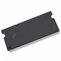
MT48LC4M32B2P-6:G Micron Technology Inc, MT48LC4M32B2P-6:G Datasheet - Page 13

MT48LC4M32B2P-6:G
Manufacturer Part Number
MT48LC4M32B2P-6:G
Description
IC SDRAM 128MBIT 167MHZ 86TSOP
Manufacturer
Micron Technology Inc
Type
SDRAMr
Datasheet
1.MT48LC4M32B2P-7G_TR.pdf
(67 pages)
Specifications of MT48LC4M32B2P-6:G
Package / Case
86-TSOPII
Format - Memory
RAM
Memory Type
SDRAM
Memory Size
128M (4Mx32)
Speed
167MHz
Interface
Parallel
Voltage - Supply
3 V ~ 3.6 V
Operating Temperature
0°C ~ 70°C
Access Time
RoHS Compliant
Memory Case Style
TSOP
No. Of Pins
86
Operating Temperature Range
0°C To +70°C
Operating Temperature Max
70°C
Operating Temperature Min
0°C
Organization
4Mx32
Density
128Mb
Address Bus
14b
Access Time (max)
17/7.5/5.5ns
Maximum Clock Rate
166MHz
Operating Supply Voltage (typ)
3.3V
Package Type
TSOP-II
Operating Temp Range
0C to 70C
Operating Supply Voltage (max)
3.6V
Operating Supply Voltage (min)
3V
Supply Current
195mA
Pin Count
86
Mounting
Surface Mount
Operating Temperature Classification
Commercial
Memory Configuration
4 BLK (1M X 32)
Interface Type
LVTTL
Rohs Compliant
Yes
Lead Free Status / RoHS Status
Lead free / RoHS Compliant
Available stocks
Company
Part Number
Manufacturer
Quantity
Price
Company:
Part Number:
MT48LC4M32B2P-6:G
Manufacturer:
MICRON
Quantity:
7 100
Company:
Part Number:
MT48LC4M32B2P-6:G
Manufacturer:
MICRON
Quantity:
4 000
Company:
Part Number:
MT48LC4M32B2P-6:G
Manufacturer:
TI
Quantity:
50
Company:
Part Number:
MT48LC4M32B2P-6:G
Manufacturer:
MICRON32
Quantity:
1 036
Part Number:
MT48LC4M32B2P-6:G
Manufacturer:
MICRON/美光
Quantity:
20 000
Burst Type
Figure 4:
PDF: 09005aef80872800/Source: 09005aef80863355
128MbSDRAMx32_2.fm - Rev. L 1/09 EN
Mode Register Definition
M8
0
–
M9
0
1
M7
0
–
Reserved states should not be used, as unknown operation or incompatibility with
future versions may result.
When a READ or WRITE command is issued, a block of columns equal to BL is effectively
selected. All accesses for that burst take place within this block, meaning that the burst
will wrap within the block if a boundary is reached. The block is uniquely selected by A1–
A7 when BL = 2; by A2–A7 when BL = 4; and by A3–A7 when BL = 8. The remaining (least
significant) address bit(s) is (are) used to select the starting location within the block.
Full-page bursts wrap within the page if the boundary is reached.
Accesses within a given burst may be programmed to be either sequential or interleaved;
this is referred to as the burst type and is selected via bit M3.
The ordering of accesses within a burst is determined by BL, the burst type and the
starting column address, as shown in Table 6 on page 14.
M11, M10, BA0, BA1 = “0”
Programmed Burst Length
M6–M0
Defined
Single Location Access
to ensure compatibility
–
Write Burst Mode
with future devices.
Operating Mode
Standard Operation
All other states reserved
Program
Reserved WB
11
A11
10
A10
M6
0
0
0
0
1
1
1
1
9
A9
M5
Op Mode
0
0
1
1
0
0
1
1
8
A8
M4
0
1
0
1
0
1
0
1
7
A7
13
CAS Latency
6
A6
CAS Latency
5
Reserved
Reserved
Reserved
Reserved
Reserved
A5
1
2
3
4
Micron Technology, Inc., reserves the right to change products or specifications without notice.
A4
M3
BT
0
1
3
A3
A2
0
0
0
0
1
1
1
1
Burst Length
2
A2
A1
0
0
1
1
0
0
1
1
A0
1
0
1
0
1
0
1
0
1
A1
0
A0
Reserved
Reserved
Reserved
Full Page
M3 = 0
Burst Type
Interleaved
Sequential
1
2
4
8
Mode Register (Ax)
Address Bus
Burst Length
©2001 Micron Technology, Inc. All rights reserved.
128Mb: x32 SDRAM
Register Definition
Reserved
Reserved
Reserved
Reserved
M3 = 1
1
2
4
8


