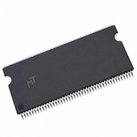
MT48LC4M32B2P-6:G Micron Technology Inc, MT48LC4M32B2P-6:G Datasheet - Page 31

MT48LC4M32B2P-6:G
Manufacturer Part Number
MT48LC4M32B2P-6:G
Description
IC SDRAM 128MBIT 167MHZ 86TSOP
Manufacturer
Micron Technology Inc
Type
SDRAMr
Datasheet
1.MT48LC4M32B2P-7G_TR.pdf
(67 pages)
Specifications of MT48LC4M32B2P-6:G
Package / Case
86-TSOPII
Format - Memory
RAM
Memory Type
SDRAM
Memory Size
128M (4Mx32)
Speed
167MHz
Interface
Parallel
Voltage - Supply
3 V ~ 3.6 V
Operating Temperature
0°C ~ 70°C
Access Time
RoHS Compliant
Memory Case Style
TSOP
No. Of Pins
86
Operating Temperature Range
0°C To +70°C
Operating Temperature Max
70°C
Operating Temperature Min
0°C
Organization
4Mx32
Density
128Mb
Address Bus
14b
Access Time (max)
17/7.5/5.5ns
Maximum Clock Rate
166MHz
Operating Supply Voltage (typ)
3.3V
Package Type
TSOP-II
Operating Temp Range
0C to 70C
Operating Supply Voltage (max)
3.6V
Operating Supply Voltage (min)
3V
Supply Current
195mA
Pin Count
86
Mounting
Surface Mount
Operating Temperature Classification
Commercial
Memory Configuration
4 BLK (1M X 32)
Interface Type
LVTTL
Rohs Compliant
Yes
Lead Free Status / RoHS Status
Lead free / RoHS Compliant
Available stocks
Company
Part Number
Manufacturer
Quantity
Price
Company:
Part Number:
MT48LC4M32B2P-6:G
Manufacturer:
MICRON
Quantity:
7 100
Company:
Part Number:
MT48LC4M32B2P-6:G
Manufacturer:
MICRON
Quantity:
4 000
Company:
Part Number:
MT48LC4M32B2P-6:G
Manufacturer:
TI
Quantity:
50
Company:
Part Number:
MT48LC4M32B2P-6:G
Manufacturer:
MICRON32
Quantity:
1 036
Part Number:
MT48LC4M32B2P-6:G
Manufacturer:
MICRON/美光
Quantity:
20 000
Figure 21:
Figure 22:
PDF: 09005aef80872800/Source: 09005aef80863355
128MbSDRAMx32_2.fm - Rev. L 1/09 EN
WRITE-to-PRECHARGE
Terminating a WRITE Burst
Notes:
Notes:
COMMAND
COMMAND
1. DQM could remain LOW in this example if the WRITE burst is a fixed length of two.
Fixed-length or full-page WRITE bursts can be truncated with the BURST TERMINATE
command. When truncating a WRITE burst, the input data applied coincident with the
BURST TERMINATE command will be ignored. The last data written (provided that
DQM is LOW at that time) will be the input data applied one clock previous to the
BURST TERMINATE command. This is shown in Figure 22, where data n is the last
desired data element of a longer burst.
COMMAND
1. DQMs are LOW.
t
t
WR = 1 CLK (
WR = 2 CLK (when
ADDRESS
ADDRESS
ADDRESS
DQM
DQM
CLK
CLK
DQ
DQ
DQ
t
CK >
BANK a,
BANK a,
BANK,
WRITE
WRITE
WRITE
COL n
COL n
COL n
D
D
D
T0
T0
n
n
n
IN
IN
IN
t
t
WR)
WR >
TERMINATE
t
BURST
n + 1
n + 1
NOP
NOP
CK)
D
D
T1
T1
IN
IN
t
WR
DON’T CARE
PRECHARGE
COMMAND
(ADDRESS)
(a or all)
(DATA)
BANK
NOP
T2
T2
NEXT
t
31
WR
PRECHARGE
(a or all)
BANK
T3
NOP
t RP
Micron Technology, Inc., reserves the right to change products or specifications without notice.
NOP
NOP
T4
t RP
BANK a,
ACTIVE
NOP
ROW
T5
DON’T CARE
BANK a,
ACTIVE
ROW
NOP
T6
©2001 Micron Technology, Inc. All rights reserved.
128Mb: x32 SDRAM
Register Definition


