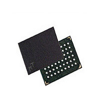
MT48H16M16LFBF-75:H Micron Technology Inc, MT48H16M16LFBF-75:H Datasheet - Page 12

MT48H16M16LFBF-75:H
Manufacturer Part Number
MT48H16M16LFBF-75:H
Description
SDRAM 256M-BIT 1.8V 54-PIN VFBGA
Manufacturer
Micron Technology Inc
Type
Mobile SDRAMr
Datasheet
1.MT48H16M16LFBF-75H.pdf
(86 pages)
Specifications of MT48H16M16LFBF-75:H
Format - Memory
RAM
Memory Type
Mobile SDRAM
Memory Size
256M (16Mx16)
Speed
132MHz
Interface
Parallel
Voltage - Supply
1.7 V ~ 1.95 V
Operating Temperature
0°C ~ 70°C
Package / Case
54-VFBGA
Organization
16Mx16
Density
256Mb
Address Bus
15b
Access Time (max)
8/6ns
Maximum Clock Rate
133MHz
Operating Supply Voltage (typ)
1.8V
Package Type
VFBGA
Operating Temp Range
0C to 70C
Operating Supply Voltage (max)
1.95V
Operating Supply Voltage (min)
1.7V
Supply Current
80mA
Pin Count
54
Mounting
Surface Mount
Operating Temperature Classification
Commercial
Lead Free Status / RoHS Status
Lead free / RoHS Compliant
Other names
Q4707290
Available stocks
Company
Part Number
Manufacturer
Quantity
Price
Company:
Part Number:
MT48H16M16LFBF-75:H
Manufacturer:
MICRON
Quantity:
5 000
Company:
Part Number:
MT48H16M16LFBF-75:H
Manufacturer:
MICRON
Quantity:
5 520
Company:
Part Number:
MT48H16M16LFBF-75:H
Manufacturer:
Micron Technology Inc
Quantity:
10 000
Part Number:
MT48H16M16LFBF-75:H
Manufacturer:
MICRON/美光
Quantity:
20 000
Table 3: VFBGA Ball Descriptions
PDF: 09005aef834c13d2
256mb_mobile_sdram_y36n.pdf - Rev. I 11/09 EN
CAS#, RAS#,
LDQM,UDQ
M(54-ball)
DQM[3:0]
BA0, BA1
DQ[31:0]
Symbol
(90-ball)
A[13:0]
V
WE#
DNU
V
CKE
CLK
V
CS#
V
NC
DDQ
SSQ
DD
SS
Supply
Supply
Supply
Supply
Type
Input
Input
Input
Input
Input
Input
Input
I/O
–
–
Note:
Description
Clock: CLK is driven by the system clock. All SDRAM input signals are sampled on the positive
edge of CLK. CLK also increments the internal burst counter and controls the output registers.
Clock enable: CKE activates (HIGH) and deactivates (LOW) the CLK signal. Deactivating the
clock provides precharge power-down and SELF REFRESH operation (all banks idle), active
power-down (row active in any bank), deep power-down (all banks idle), or CLOCK SUSPEND
operation (burst/access in progress). CKE is synchronous except after the device enters power-
down and self refresh modes, where CKE becomes asynchronous until after exiting the same
mode. The input buffers, including CLK, are disabled during power-down and self refresh
modes, providing low standby power.
Chip select: CS# enables (registered LOW) and disables (registered HIGH) the command decod-
er. All commands are masked when CS# is registered HIGH. CS# provides for external bank
selection on systems with multiple banks. CS# is considered part of the command code.
Command inputs: RAS#, CAS#, and WE# (along with CS#) define the command being entered.
Input/Output mask: DQM is sampled HIGH and is an input mask signal for write accesses and
an output enable signal for read accesses. Input data is masked during a WRITE cycle. The
output buffers are High-Z (two-clock latency) during a READ cycle. For the x16, LDQM corre-
sponds to DQ[7:0] and UDQM corresponds to DQ[16:8]. For the x32, DQM0 corresponds to
DQ[7:0], DQM1 corresponds to DQ[15:8], DQM2 corresponds to DQ[23:16], and DQM3 corre-
sponds to DQ[31:24]. DQM[3:0] (or LDQM and UDQM if x16) are considered same state when
referenced as DQM.
Bank address input(s): BA0 and BA1 define to which bank the ACTIVE, READ, WRITE, or PRE-
CHARGE command is being applied. BA0 and BA1 become “Don’t Care” when registering an
ALL BANK PRECHARGE (A10 HIGH).
Address inputs: Addresses are sampled during the ACTIVE command (row) and READ/WRITE
command [column); column address A[9:0] (x16); with A10 defining auto precharge] to select
one location out of the memory array in the respective bank. A10 is sampled during a PRE-
CHARGE command to determine if all banks are to be precharged (A10 HIGH) or bank
selected by BA0, BA1. The address inputs also provide the op-code during a LOAD MODE REG-
ISTER command. The maximum address range is dependent upon configuration. Unused
address pins become RFU.
Data input/output: Data bus.
DQ power: Provide isolated power to DQ for improved noise immunity.
DQ ground: Provide isolated ground to DQ for improved noise immunity.
Core power supply.
Ground.
Do not use: Must be grounded or left floating.
Internally not connected. These balls can be left unconnected but it is recommended that
they be connected to V
1. Balls marked RFU may or may not be connected internally. These balls should not be
used. Contact the factory for details.
SS
256Mb: 16 Meg x 16, 8 Meg x 32 Mobile SDRAM
.
1
12
Micron Technology, Inc. reserves the right to change products or specifications without notice.
Ball Assignments and Descriptions
©2008 Micron Technology, Inc. All rights reserved.


