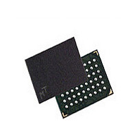
MT48H16M16LFBF-75:H Micron Technology Inc, MT48H16M16LFBF-75:H Datasheet - Page 26

MT48H16M16LFBF-75:H
Manufacturer Part Number
MT48H16M16LFBF-75:H
Description
SDRAM 256M-BIT 1.8V 54-PIN VFBGA
Manufacturer
Micron Technology Inc
Type
Mobile SDRAMr
Datasheet
1.MT48H16M16LFBF-75H.pdf
(86 pages)
Specifications of MT48H16M16LFBF-75:H
Format - Memory
RAM
Memory Type
Mobile SDRAM
Memory Size
256M (16Mx16)
Speed
132MHz
Interface
Parallel
Voltage - Supply
1.7 V ~ 1.95 V
Operating Temperature
0°C ~ 70°C
Package / Case
54-VFBGA
Organization
16Mx16
Density
256Mb
Address Bus
15b
Access Time (max)
8/6ns
Maximum Clock Rate
133MHz
Operating Supply Voltage (typ)
1.8V
Package Type
VFBGA
Operating Temp Range
0C to 70C
Operating Supply Voltage (max)
1.95V
Operating Supply Voltage (min)
1.7V
Supply Current
80mA
Pin Count
54
Mounting
Surface Mount
Operating Temperature Classification
Commercial
Lead Free Status / RoHS Status
Lead free / RoHS Compliant
Other names
Q4707290
Available stocks
Company
Part Number
Manufacturer
Quantity
Price
Company:
Part Number:
MT48H16M16LFBF-75:H
Manufacturer:
MICRON
Quantity:
5 000
Company:
Part Number:
MT48H16M16LFBF-75:H
Manufacturer:
MICRON
Quantity:
5 520
Company:
Part Number:
MT48H16M16LFBF-75:H
Manufacturer:
Micron Technology Inc
Quantity:
10 000
Part Number:
MT48H16M16LFBF-75:H
Manufacturer:
MICRON/美光
Quantity:
20 000
Functional Description
PDF: 09005aef834c13d2
256mb_mobile_sdram_y36n.pdf - Rev. I 11/09 EN
Mobile LPSDR devices are quad-bank DRAM that operate at 1.8V and include a synchro-
nous interface. All signals are registered on the positive edge of the clock signal, CLK.
Read and write accesses to the device are burst oriented; accesses start at a selected
location and continue for a programmed number of locations in a programmed se-
quence. Accesses begin with the registration of an ACTIVE command, followed by a
READ or WRITE command. The address bits registered coincident with the ACTIVE com-
mand are used to select the bank and row to be accessed (BA0 and BA1 select the bank).
The address bits registered coincident with the READ or WRITE command are used to
select the starting column location for the burst access.
The device provides for programmable READ or WRITE burst lengths. An auto pre-
charge function may be enabled to provide a self-timed row precharge that is initiated
at the end of the burst sequence.
The device uses an internal pipelined architecture that enables changing the column
address on every clock cycle to achieve high-speed, fully random access. Precharging
one bank while accessing one of the other three banks will hide the precharge cycles.
The device is designed to operate in 1.8V memory systems. An auto refresh mode is pro-
vided, along with power-saving, power-down, and deep power-down modes. All inputs
and outputs are LVTTL-compatible.
The device offers substantial advances in DRAM operating performance, including the
ability to synchronously burst data at a high data rate with automatic column-address
generation, the ability to interleave between internal banks in order to hide precharge
time, and the capability to randomly change column addresses on each clock cycle dur-
ing a burst access.
256Mb: 16 Meg x 16, 8 Meg x 32 Mobile SDRAM
26
Micron Technology, Inc. reserves the right to change products or specifications without notice.
Functional Description
©2008 Micron Technology, Inc. All rights reserved.


