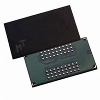
MT48V8M16LFB4-8:G Micron Technology Inc, MT48V8M16LFB4-8:G Datasheet - Page 24

MT48V8M16LFB4-8:G
Manufacturer Part Number
MT48V8M16LFB4-8:G
Description
IC SDRAM 128MBIT 125MHZ 54VFBGA
Manufacturer
Micron Technology Inc
Type
Mobile SDRAMr
Specifications of MT48V8M16LFB4-8:G
Format - Memory
RAM
Memory Type
Mobile SDRAM
Memory Size
128M (8Mx16)
Speed
125MHz
Interface
Parallel
Voltage - Supply
2.3 V ~ 2.7 V
Operating Temperature
0°C ~ 70°C
Package / Case
54-VFBGA
Organization
8Mx16
Density
128Mb
Address Bus
14b
Access Time (max)
19/8/7ns
Maximum Clock Rate
125MHz
Operating Supply Voltage (typ)
2.5V
Package Type
VFBGA
Operating Temp Range
0C to 70C
Operating Supply Voltage (max)
2.7V
Operating Supply Voltage (min)
2.3V
Supply Current
100mA
Pin Count
54
Mounting
Surface Mount
Operating Temperature Classification
Commercial
Lead Free Status / RoHS Status
Lead free / RoHS Compliant
Available stocks
Company
Part Number
Manufacturer
Quantity
Price
Company:
Part Number:
MT48V8M16LFB4-8:G
Manufacturer:
MICRON
Quantity:
4 000
Company:
Part Number:
MT48V8M16LFB4-8:G
Manufacturer:
Micron Technology Inc
Quantity:
10 000
Company:
Part Number:
MT48V8M16LFB4-8:G TR
Manufacturer:
Micron Technology Inc
Quantity:
10 000
LOAD MODE REGISTER
ACTIVE
READ
WRITE
PRECHARGE
Auto Precharge
PDF: 09005aef807f4885/Source: 09005aef8071a76b
128Mbx16x32Mobile_2.fm - Rev. M 1/09 EN
The mode register is loaded via inputs A0–A11. Refer to “Mode Register Definition” on
page 18. The LOAD MODE REGISTER and LOAD EXTENDED MODE REGISTER
commands can only be issued when all banks are idle, and a subsequent executable
command cannot be issued until
The ACTIVE command is used to open (or activate) a row in a particular bank for a
subsequent access. The value on the BA0, BA1 inputs selects the bank, and the address
provided on inputs A0–A11 selects the row. This row remains active (or open) for
accesses until a PRECHARGE command is issued to that bank. A PRECHARGE
command must be issued before opening a different row in the same bank.
The READ command is used to initiate a burst read access to an active row. The value on
the BA0, BA1 inputs selects the bank, and the address provided on inputs A0–A8 (x16) or
A0–A7 (x32) selects the starting column location. The value on input A10 determines
whether auto precharge is used. If auto precharge is selected, the row being accessed will
be precharged at the end of the read burst; if auto precharge is not selected, the row will
remain open for subsequent accesses. Read data appears on the DQ subject to the logic
level on the DQM inputs two clocks earlier. If a given DQM signal was registered HIGH,
the corresponding DQ will be High-Z two clocks later; if the DQM signal was registered
LOW, the DQ will provide valid data.
The WRITE command is used to initiate a burst write access to an active row. The value
on the BA0, BA1 inputs selects the bank, and the address provided on inputs A0–A8 (x16)
or A0–A7 (x32) selects the starting column location. The value on input A10 determines
whether auto precharge is used. If auto precharge is selected, the row being accessed will
be precharged at the end of the write burst; if auto precharge is not selected, the row will
remain open for subsequent accesses. Input data appearing on the DQ is written to the
memory array subject to the DQM input logic level appearing coincident with the data.
If a given DQM signal is registered LOW, the corresponding data will be written to
memory; if the DQM signal is registered HIGH, the corresponding data inputs will be
ignored, and a write will not be executed to that byte/column location.
The PRECHARGE command is used to deactivate the open row in a particular bank or
the open row in all banks. The bank(s) will be available for a subsequent row access a
specified time (
whether one or all banks are to be precharged, and in the case where only one bank is to
be precharged, inputs BA0, BA1 select the bank. Otherwise BA0, BA1 are treated as
“Don’t Care.” After a bank has been precharged, it is in the idle state and must be acti-
vated prior to any READ or WRITE commands being issued to that bank.
Auto precharge is a feature that performs the same individual-bank precharge function
described above, without requiring an explicit command. This is accomplished by using
A10 to enable auto precharge in conjunction with a specific READ or WRITE command.
A precharge of the bank/row that is addressed with the READ or WRITE command is
t
RP) after the PRECHARGE command is issued. Input A10 determines
24
t
MRD is met.
Micron Technology, Inc., reserves the right to change products or specifications without notice.
128Mb: x16, x32 Mobile SDRAM
©2001 Micron Technology, Inc. All rights reserved.
Register Definition


