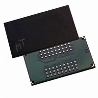
MT48V8M16LFB4-8:G Micron Technology Inc, MT48V8M16LFB4-8:G Datasheet - Page 36

MT48V8M16LFB4-8:G
Manufacturer Part Number
MT48V8M16LFB4-8:G
Description
IC SDRAM 128MBIT 125MHZ 54VFBGA
Manufacturer
Micron Technology Inc
Type
Mobile SDRAMr
Specifications of MT48V8M16LFB4-8:G
Format - Memory
RAM
Memory Type
Mobile SDRAM
Memory Size
128M (8Mx16)
Speed
125MHz
Interface
Parallel
Voltage - Supply
2.3 V ~ 2.7 V
Operating Temperature
0°C ~ 70°C
Package / Case
54-VFBGA
Organization
8Mx16
Density
128Mb
Address Bus
14b
Access Time (max)
19/8/7ns
Maximum Clock Rate
125MHz
Operating Supply Voltage (typ)
2.5V
Package Type
VFBGA
Operating Temp Range
0C to 70C
Operating Supply Voltage (max)
2.7V
Operating Supply Voltage (min)
2.3V
Supply Current
100mA
Pin Count
54
Mounting
Surface Mount
Operating Temperature Classification
Commercial
Lead Free Status / RoHS Status
Lead free / RoHS Compliant
Available stocks
Company
Part Number
Manufacturer
Quantity
Price
Company:
Part Number:
MT48V8M16LFB4-8:G
Manufacturer:
MICRON
Quantity:
4 000
Company:
Part Number:
MT48V8M16LFB4-8:G
Manufacturer:
Micron Technology Inc
Quantity:
10 000
Company:
Part Number:
MT48V8M16LFB4-8:G TR
Manufacturer:
Micron Technology Inc
Quantity:
10 000
Figure 21:
Figure 22:
PDF: 09005aef807f4885/Source: 09005aef8071a76b
128Mbx16x32Mobile_2.fm - Rev. M 1/09 EN
WRITE Burst
WRITE-to-WRITE
Notes:
Notes:
COMMAND
1. BL = 2. DQM is LOW.
COMMAND
1. DQM is LOW. Each WRITE command may be to any bank.
Data for any WRITE burst may be truncated with a subsequent READ command, and
data for a fixed-length WRITE burst may be immediately followed by a READ command.
After the READ command is registered, the data inputs will be ignored, and writes will
not be executed. An example is shown in Figure 24 on page 37. Data n + 1 is either the
last of a burst of two or the last desired of a longer burst.
Data for a fixed-length WRITE burst may be followed by, or truncated with, a
PRECHARGE command to the same bank (provided that auto precharge was not acti-
vated), and a full-page WRITE burst may be truncated with a PRECHARGE command to
the same bank. The PRECHARGE command should be issued
which the last desired input data element is registered. The auto precharge mode
requires a
In addition, when truncating a WRITE burst, the DQM signal must be used to mask
input data for the clock edge prior to, and the clock edge coincident with, the
PRECHARGE command. An example is shown in Figure 25 on page 38. Data n + 1 is
either the last of a burst of two or the last desired of a longer burst. Following the
PRECHARGE command, a subsequent command to the same bank cannot be issued
until
Figure 25 on page 38).
ADDRESS
ADDRESS
TRANSITIONING DATA
t
CLK
CLK
DQ
DQ
RP is met. The PRECHARGE can be issued coincident with the second clock (see
t
TRANSITIONING DATA
WR of at least one clock plus time, regardless of frequency.
WRITE
BANK,
COL n
WRITE
BANK,
COL n
T0
D
D
T0
n
n
IN
IN
NOP
n + 1
n + 1
T1
NOP
D
T1
D
IN
IN
DON’T CARE
WRITE
BANK,
NOP
COL b
T2
T2
D
b
IN
36
DON’T CARE
T3
NOP
Micron Technology, Inc., reserves the right to change products or specifications without notice.
128Mb: x16, x32 Mobile SDRAM
t
WR after the clock edge at
©2001 Micron Technology, Inc. All rights reserved.
READs


