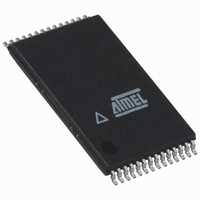
AT45DB642D-TU Atmel, AT45DB642D-TU Datasheet - Page 16

AT45DB642D-TU
Manufacturer Part Number
AT45DB642D-TU
Description
IC FLASH 64MBIT 66MHZ 28TSOP
Manufacturer
Atmel
Datasheet
1.AT45DB642D-CU.pdf
(58 pages)
Specifications of AT45DB642D-TU
Format - Memory
FLASH
Memory Type
DataFLASH
Memory Size
64M (8192 pages x 1056 bytes)
Speed
66MHz
Interface
Parallel/Serial
Voltage - Supply
2.7 V ~ 3.6 V
Operating Temperature
-40°C ~ 85°C
Package / Case
28-TSOP
Density
64Mb
Access Time (max)
6ns
Interface Type
Parallel/Serial-SPI
Boot Type
Not Required
Address Bus
1/8Bit
Operating Supply Voltage (typ)
3.3V
Operating Temp Range
-40C to 85C
Package Type
TSOP-I
Program/erase Volt (typ)
2.7 to 3.6V
Sync/async
Synchronous
Operating Temperature Classification
Industrial
Operating Supply Voltage (min)
2.7V
Operating Supply Voltage (max)
3.6V
Word Size
8b
Number Of Words
8M
Supply Current
15mA
Mounting
Surface Mount
Pin Count
28
Data Bus Width
8 bit
Architecture
Sectored
Supply Voltage (max)
3.6 V
Supply Voltage (min)
2.7 V
Maximum Operating Current
15 mA
Mounting Style
SMD/SMT
Organization
256 KB x 32
Memory Configuration
8192 Pages X 1056 Bytes
Clock Frequency
66MHz
Supply Voltage Range
2.7V To 3.6V
Memory Case Style
TSOP
Rohs Compliant
Yes
Lead Free Status / RoHS Status
Lead free / RoHS Compliant
Available stocks
Company
Part Number
Manufacturer
Quantity
Price
Company:
Part Number:
AT45DB642D-TU
Manufacturer:
MICRON
Quantity:
101
Company:
Part Number:
AT45DB642D-TU
Manufacturer:
ATMEL
Quantity:
9 396
Company:
Part Number:
AT45DB642D-TU
Manufacturer:
AT
Quantity:
5
Part Number:
AT45DB642D-TU
Manufacturer:
ATMEL/爱特梅尔
Quantity:
20 000
9.1.2
16
AT45DB642D
Program Sector Protection Register Command
the register can be reprogrammed, then the erroneous program or erase command will not be
processed because all sectors would be protected.
Figure 9-2.
Once the Sector Protection Register has been erased, it can be reprogrammed using the Pro-
gram Sector Protection Register command.
To program the Sector Protection Register, the CS pin must first be asserted and the appropri-
ate 4-byte opcode sequence must be clocked into the device via the SI or I/O7 - I/O0 pin. The 4-
byte opcode sequence must start with 3DH and be followed by 2AH, 7FH, and FCH. After the
last bit of the opcode sequence has been clocked into the device, the data for the contents of the
Sector Protection Register must be clocked in. As described in
tion Register contains 32 bytes of data, so 32 bytes must be clocked into the device. The first
byte of data corresponds to sector 0, the second byte corresponds to sector 1, and so on with
the last byte of data corresponding to sector 31.
After the last data byte has been clocked in, the CS pin must be deasserted to initiate the inter-
nally self-timed program cycle. The programming of the Sector Protection Register should take
place in a time of t
the device is powered-down during the program cycle, then the contents of the Sector Protection
Register cannot be guaranteed.
If the proper number of data bytes is not clocked in before the CS pin is deasserted, then the
protection status of the sectors corresponding to the bytes not clocked in can not be guaranteed.
For example, if only the first two bytes are clocked in instead of the complete 32 bytes, then the
protection status of the last 30 sectors cannot be guaranteed. Furthermore, if more than 32
bytes of data is clocked into the device, then the data will wrap back around to the beginning of
the register. For instance, if 33 bytes of data are clocked in, then the 33rd byte will be stored at
byte location 0 of the Sector Protection Register.
If a value other than 00H or FFH is clocked into a byte location of the Sector Protection Register,
then the protection status of the sector corresponding to that byte location cannot be guaran-
teed. For example, if a value of 17H is clocked into byte location 2 of the Sector Protection
Register, then the protection status of sector 2 cannot be guaranteed.
The Sector Protection Register can be reprogrammed while the sector protection enabled or dis-
abled. Being able to reprogram the Sector Protection Register with the sector protection enabled
allows the user to temporarily disable the sector protection to an individual sector rather than dis-
abling sector protection completely.
Command
Erase Sector Protection Register
SI or IO
Erase Sector Protection Register
7
P
- IO
, during which time the Status Register will indicate that the device is busy. If
CS
0
Each transition
represents 8 bits
Opcode
Byte 1
Byte 1
3DH
Opcode
Byte 2
Byte 2
2AH
Opcode
Byte 3
Section
Opcode
Byte 4
Byte 3
7FH
9.1, the Sector Protec-
3542K–DFLASH–04/09
Byte 4
CFH


