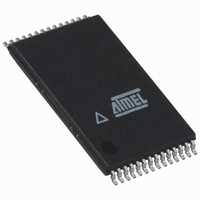
AT45DB642D-TU Atmel, AT45DB642D-TU Datasheet - Page 4

AT45DB642D-TU
Manufacturer Part Number
AT45DB642D-TU
Description
IC FLASH 64MBIT 66MHZ 28TSOP
Manufacturer
Atmel
Datasheet
1.AT45DB642D-CU.pdf
(58 pages)
Specifications of AT45DB642D-TU
Format - Memory
FLASH
Memory Type
DataFLASH
Memory Size
64M (8192 pages x 1056 bytes)
Speed
66MHz
Interface
Parallel/Serial
Voltage - Supply
2.7 V ~ 3.6 V
Operating Temperature
-40°C ~ 85°C
Package / Case
28-TSOP
Density
64Mb
Access Time (max)
6ns
Interface Type
Parallel/Serial-SPI
Boot Type
Not Required
Address Bus
1/8Bit
Operating Supply Voltage (typ)
3.3V
Operating Temp Range
-40C to 85C
Package Type
TSOP-I
Program/erase Volt (typ)
2.7 to 3.6V
Sync/async
Synchronous
Operating Temperature Classification
Industrial
Operating Supply Voltage (min)
2.7V
Operating Supply Voltage (max)
3.6V
Word Size
8b
Number Of Words
8M
Supply Current
15mA
Mounting
Surface Mount
Pin Count
28
Data Bus Width
8 bit
Architecture
Sectored
Supply Voltage (max)
3.6 V
Supply Voltage (min)
2.7 V
Maximum Operating Current
15 mA
Mounting Style
SMD/SMT
Organization
256 KB x 32
Memory Configuration
8192 Pages X 1056 Bytes
Clock Frequency
66MHz
Supply Voltage Range
2.7V To 3.6V
Memory Case Style
TSOP
Rohs Compliant
Yes
Lead Free Status / RoHS Status
Lead free / RoHS Compliant
Available stocks
Company
Part Number
Manufacturer
Quantity
Price
Company:
Part Number:
AT45DB642D-TU
Manufacturer:
MICRON
Quantity:
101
Company:
Part Number:
AT45DB642D-TU
Manufacturer:
ATMEL
Quantity:
9 396
Company:
Part Number:
AT45DB642D-TU
Manufacturer:
AT
Quantity:
5
Part Number:
AT45DB642D-TU
Manufacturer:
ATMEL/爱特梅尔
Quantity:
20 000
Table 2-1.
4
Symbol
SER/BYTE
V
GND
V
GNDP
Figure 2-1.
CC
CCP
RDY/BUSY
SCK/CLK
RESET
GND
VCC
AT45DB642D
WP
NC
NC
NC
NC
NC
SO
CS
SI
Name and Function
Serial/8-bit Interface Control: The DataFlash may be configured to utilize either its serial port or
8-bit port through the use of the serial/8-bit control pin (SER/BYTE). When the SER/BYTE pin is
held high, the serial port (SI and SO) of the DataFlash will be used for all data transfers, and the
8-bit port (I/O7 - I/O0) will be in a high impedance state. Any data presented on the 8-bit port
while SER/BYTE is held high will be ignored. When the SER/BYTE is held low, the 8-bit port will
be used for all data transfers, and the SO pin of the serial port will be in a high impedance state.
While SER/BYTE is low, any data presented on the SI pin will be ignored. Switching between the
serial port and 8-bit port should only be done while the CS pin is high and the device is not busy
in an internally self-timed operation.
The SER/BYTE pin is internally pulled high; therefore, if the 8-bit port is never to be used, then
connection of the SER/BYTE pin is not necessary. In addition, if the SER/BYTE pin is not
connected or if the SER/BYTE pin is always driven high externally, then the 8-bit input/output pins
(I/O7-I/O0), the VCCP pin, and the GNDP pin should be treated as “no connect”.
Device Power Supply: The V
Operations at invalid V
Ground: The ground reference for the power supply. GND should be connected to the system
ground.
8-bit Port Supply Voltage: The VCCP pin is used to supply power for the 8-bit input/output pins
(I/O7-I/O0). The VCCP pin needs to be used if the 8-bit port is to be utilized; however, this pin
should be treated as “no connect” if the SER/BYTE pin is not connected or if the SER/BYTE pin is
always driven high externally.
8-bit Port Ground: The GNDP pin is used to provide ground for the 8-bit input/output pins (I/O7-
I/O0). The GNDP pin needs to be used if the 8-bit port is to be utilized; however, this pin should
be treated as “no connect” if the SER/BYTE pin is not connected or if the SER/BYTE pin is
always driven high externally.
Pin Configurations (Continued)
1
2
3
4
5
6
7
8
9
10
11
12
13
14
TSOP Top View: Type 1
CC
voltages may produce spurious results and should not be attempted.
CC
pin is used to supply the source voltage to the device.
28
27
26
25
24
23
22
21
20
19
18
17
16
15
NC
NC
I/O7
I/O6
I/O5
I/O4
VCCP
GNDP
I/O3
I/O2
I/O1
I/O0
SER/BYTE
NC
Figure 2-2.
Figure 2-3.
A
B
C
D
E
BGA Package Ball-Out (Top View)
CASON Top View through Package
RESET
SCK
CS
NC
NC
NC
NC
1
SI
1
2
3
4
SCK
NC
CS
SO
NC
2
RDY/BSY
GND
NC
NC
3
SI
RESET
VCC
NC
WP
NC
4
8
7
6
5
SO
GND
VCC
WP
NC
NC
NC
NC
NC
5
Asserted
State
3542K–DFLASH–04/09
Low
–
–
–
–
Ground
Ground
Power
Power
Type
Input


