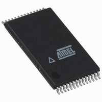
AT45DB642D-TU Atmel, AT45DB642D-TU Datasheet - Page 5

AT45DB642D-TU
Manufacturer Part Number
AT45DB642D-TU
Description
IC FLASH 64MBIT 66MHZ 28TSOP
Manufacturer
Atmel
Datasheet
1.AT45DB642D-CU.pdf
(58 pages)
Specifications of AT45DB642D-TU
Format - Memory
FLASH
Memory Type
DataFLASH
Memory Size
64M (8192 pages x 1056 bytes)
Speed
66MHz
Interface
Parallel/Serial
Voltage - Supply
2.7 V ~ 3.6 V
Operating Temperature
-40°C ~ 85°C
Package / Case
28-TSOP
Density
64Mb
Access Time (max)
6ns
Interface Type
Parallel/Serial-SPI
Boot Type
Not Required
Address Bus
1/8Bit
Operating Supply Voltage (typ)
3.3V
Operating Temp Range
-40C to 85C
Package Type
TSOP-I
Program/erase Volt (typ)
2.7 to 3.6V
Sync/async
Synchronous
Operating Temperature Classification
Industrial
Operating Supply Voltage (min)
2.7V
Operating Supply Voltage (max)
3.6V
Word Size
8b
Number Of Words
8M
Supply Current
15mA
Mounting
Surface Mount
Pin Count
28
Data Bus Width
8 bit
Architecture
Sectored
Supply Voltage (max)
3.6 V
Supply Voltage (min)
2.7 V
Maximum Operating Current
15 mA
Mounting Style
SMD/SMT
Organization
256 KB x 32
Memory Configuration
8192 Pages X 1056 Bytes
Clock Frequency
66MHz
Supply Voltage Range
2.7V To 3.6V
Memory Case Style
TSOP
Rohs Compliant
Yes
Lead Free Status / RoHS Status
Lead free / RoHS Compliant
Available stocks
Company
Part Number
Manufacturer
Quantity
Price
Company:
Part Number:
AT45DB642D-TU
Manufacturer:
MICRON
Quantity:
101
Company:
Part Number:
AT45DB642D-TU
Manufacturer:
ATMEL
Quantity:
9 396
Company:
Part Number:
AT45DB642D-TU
Manufacturer:
AT
Quantity:
5
Part Number:
AT45DB642D-TU
Manufacturer:
ATMEL/爱特梅尔
Quantity:
20 000
3. Block Diagram
4. Memory Array
Figure 4-1.
3542K–DFLASH–04/09
SECTOR ARCHITECTURE
SECTOR 30 = 256 Pages
SECTOR 31 = 256 Pages
SECTOR 1 = 256 Pages
SECTOR 2 = 256 Pages
SECTOR 0b = 248 Pages
262,144/270,336 bytes
262,144/270,336
262,144/270,336 bytes
SECTOR 0a = 8 Pages
262,144/270,336 bytes
253,952/261,888 bytes
8192/8,448 bytes
Memory Architecture Diagram
bytes
To provide optimal flexibility, the memory array of the AT45DB642D is divided into three levels of
granularity comprising of sectors, blocks, and pages. The “Memory Architecture Diagram” illus-
trates the breakdown of each level and details the number of pages per sector and block. All
program operations to the DataFlash occur on a page by page basis. The erase operations can
be performed at the chip, sector, block or page level.
RDY/BUSY
SER/BYTE
SCK/CLK
RESET
GND
VCC
SECTOR 0
WP
CS
BUFFER 1 (1024/1056 BYTES)
PAGE (1024/1056 BYTES)
BLOCK ARCHITECTURE
Block = 8,192/8,448 bytes
BLOCK 1022
BLOCK 1023
BLOCK 30
BLOCK 31
BLOCK 32
BLOCK 33
BLOCK 62
BLOCK 63
BLOCK 64
BLOCK 65
BLOCK 0
BLOCK 1
BLOCK 2
SI
SO
FLASH MEMORY ARRAY
I/O INTERFACE
8 Pages
BUFFER 2 (1024/1056 BYTES)
I/O7 - I/O0
PAGE ARCHITECTURE
Page = 1,024/1,056 bytes
PAGE 8,190
PAGE 8,190
PAGE 14
PAGE 15
PAGE 16
PAGE 17
PAGE 18
PAGE 0
PAGE 1
PAGE 6
PAGE 7
PAGE 8
PAGE 9
5


