EPC1PC8 Altera, EPC1PC8 Datasheet - Page 20
EPC1PC8
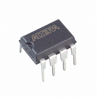
Manufacturer Part Number
EPC1PC8
Description
IC CONFIG DEVICE 1MBIT 8-DIP
Manufacturer
Altera
Series
EPCr
Datasheet
1.EPC1PC8.pdf
(26 pages)
Specifications of EPC1PC8
Programmable Type
OTP
Memory Size
1Mb
Voltage - Supply
3 V ~ 3.6 V, 4.75 V ~ 5.25 V
Operating Temperature
0°C ~ 70°C
Package / Case
8-DIP (0.300", 7.62mm)
For Use With
PLMJ1213 - PROGRAMMER ADAPTER 20 PIN J-LEAD
Lead Free Status / RoHS Status
Contains lead / RoHS non-compliant
Other names
544-1231-5
Available stocks
Company
Part Number
Manufacturer
Quantity
Price
Company:

Part Number:
EPC1PC8
Manufacturer:
INITIO
Quantity:
1 001
Company:
Part Number:
EPC1PC8
Manufacturer:
ALTERA
Quantity:
5 510
Company:
Part Number:
EPC1PC8
Manufacturer:
ALTERA41
Quantity:
5 747
Part Number:
EPC1PC8
Manufacturer:
ALTERA/阿尔特拉
Quantity:
20 000
Company:
Part Number:
EPC1PC8N
Manufacturer:
ALTERA
Quantity:
410
Part Number:
EPC1PC8N
Manufacturer:
ALTERA
Quantity:
20 000


4–20 Chapter 4: Configuration Devices for SRAM-Based LUT Devices Data Sheet
Table 4–15. EPC1064, EPC1064V, and EPC1213 Device I
Table 4–16. EPC2 Device Values
Table 4–17. EPC1 Device I
Table 4–18. EPC1441 Device I
Table 4–19. Capacitance
Configuration Handbook (Complete Two-Volume Set)
I
I
I
I
R
I
I
I
I
I
C
C
Notes to
(1) For more information, refer to the Operating Requirements for Altera Devices Data Sheet.
(2) The minimum DC input is -0.3 V. During transitions, the inputs may undershoot to -2.0 V or overshoot to 7.0 V for input currents less than 100
(3) Numbers in parentheses are for industrial temperature range devices.
(4) Maximum V
(5) Certain EPC2 pins may be driven to 5.75 V when operated with a 3.3-V V
(6) The I
(7) Capacitance is sample-tested only.
Symbol
CC0
CC1
CC0
CC1
Symbol
CC0
CC1
Symbol
CC0
CC1
CC1
Symbol
Symbol
CONF
IN
OUT
mA and periods shorter than 20 ns under no-load conditions.
Table 4–12
OH
V
V
configuration)
V
V
configuration)
V
V
configuration)
V
configuration)
Input pin capacitance
Output pin capacitance
parameter refers to high-level TTL or CMOS output current; the I
CC
CC
V
V
configuration)
Configuration pins
CC
CC
CC
CC
CC
CC
CC
CC
supply current (standby)
supply current (during
supply current (standby)
supply current (during
supply current (standby)
supply current (during
supply current (during
supply current (standby)
supply current (during
rise time is 100 ms.
through
Parameter
Parameter
Parameter
Parameter
(Note 7)
Parameter
CC
Table
Supply Current Values
CC
4–19:
Supply Current Values
V
V
V
V
V
V
V
V
Internal pull up (OE, nCS,
nINIT_CONF)
CC
CC
CC
CC
IN
OUT
CC
CC
= 0 V, f = 1.0 MHz
= 5.0 V
= 5.0 V
= 3.3 V
= 3.3 V
CC
= 5.0 V or 3.3 V
= 5.0 V or 3.3 V
= 0 V, f = 1.0 MHz
Supply Current Values
Conditions
Conditions
Conditions
Conditions
—
—
—
—
OL
CC
Conditions
. Refer to
parameter refers to low-level TTL or CMOS output current.
Table 4–4 on page
Min
Min
Min
—
—
Min
—
—
—
—
—
—
—
—
—
© December 2009
4–11.
Min
Typ
100
Typ
Typ
Typ
—
—
10
50
30
10
30
15
50
18
5
1
Operating Conditions
16.5
Max
Max
Max
Max
Max
Altera Corporation
200
100
100
50
50
—
50
30
10
10
10
60
Unit
Unit
Unit
Unit
Unit
mA
mA
mA
mA
mA
mA
k
A
µA
µA
µA
pF
pF
Related parts for EPC1PC8
Image
Part Number
Description
Manufacturer
Datasheet
Request
R

Part Number:
Description:
Configuration EPROMs For Flex Devices
Manufacturer:
Altera Corporation
Datasheet:

Part Number:
Description:
CYCLONE II STARTER KIT EP2C20N
Manufacturer:
Altera
Datasheet:

Part Number:
Description:
CPLD, EP610 Family, ECMOS Process, 300 Gates, 16 Macro Cells, 16 Reg., 16 User I/Os, 5V Supply, 35 Speed Grade, 24DIP
Manufacturer:
Altera Corporation
Datasheet:
Part Number:
Description:
CPLD, EP610 Family, ECMOS Process, 300 Gates, 16 Macro Cells, 16 Reg., 16 User I/Os, 5V Supply, 15 Speed Grade, 24DIP
Manufacturer:
Altera Corporation
Datasheet:
Part Number:
Description:
Manufacturer:
Altera Corporation
Datasheet:
Part Number:
Description:
CPLD, EP610 Family, ECMOS Process, 300 Gates, 16 Macro Cells, 16 Reg., 16 User I/Os, 5V Supply, 30 Speed Grade, 24DIP
Manufacturer:
Altera Corporation
Datasheet:
Part Number:
Description:
High-performance, low-power erasable programmable logic devices with 8 macrocells, 10ns
Manufacturer:
Altera Corporation
Datasheet:
Part Number:
Description:
High-performance, low-power erasable programmable logic devices with 8 macrocells, 7ns
Manufacturer:
Altera Corporation
Datasheet:
Part Number:
Description:
Classic EPLD
Manufacturer:
Altera Corporation
Datasheet:
Part Number:
Description:
High-performance, low-power erasable programmable logic devices with 8 macrocells, 10ns
Manufacturer:
Altera Corporation
Datasheet:
Part Number:
Description:
Manufacturer:
Altera Corporation
Datasheet:
Part Number:
Description:
Manufacturer:
Altera Corporation
Datasheet:
Part Number:
Description:
Manufacturer:
Altera Corporation
Datasheet: