EPC1PC8 Altera, EPC1PC8 Datasheet - Page 24
EPC1PC8
Manufacturer Part Number
EPC1PC8
Description
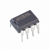
IC CONFIG DEVICE 1MBIT 8-DIP
Manufacturer
Altera
Series
EPCr
Datasheet
1.EPC1PC8.pdf
(26 pages)
Specifications of EPC1PC8
Programmable Type
OTP
Memory Size
1Mb
Voltage - Supply
3 V ~ 3.6 V, 4.75 V ~ 5.25 V
Operating Temperature
0°C ~ 70°C
Package / Case
8-DIP (0.300", 7.62mm)
For Use With
PLMJ1213 - PROGRAMMER ADAPTER 20 PIN J-LEAD
Lead Free Status / RoHS Status
Contains lead / RoHS non-compliant
Other names
544-1231-5
Available stocks
Company
Part Number
Manufacturer
Quantity
Price
Company:

Part Number:
EPC1PC8
Manufacturer:
INITIO
Quantity:
1 001
Company:
Part Number:
EPC1PC8
Manufacturer:
ALTERA
Quantity:
5 510
Company:
Part Number:
EPC1PC8
Manufacturer:
ALTERA41
Quantity:
5 747
Part Number:
EPC1PC8
Manufacturer:
ALTERA/阿尔特拉
Quantity:
20 000
Company:
Part Number:
EPC1PC8N
Manufacturer:
ALTERA
Quantity:
410
Part Number:
EPC1PC8N
Manufacturer:
ALTERA
Quantity:
20 000


4–24 Chapter 4: Configuration Devices for SRAM-Based LUT Devices Data Sheet
Package
Figure 4–6. EPC1, EPC1064, EPC1064V, EPC1213, and EPC1441 Package Pin-Out Diagrams
Notes to
(1) EPC1 and EPC1441 devices are one-time programmable devices. ISP is not available in these devices.
(2) The
Figure 4–7. EPC2 Package Pin-Out Diagrams
Configuration Handbook (Complete Two-Volume Set)
be left unconnected.
nCASC
Figure
DCLK
DATA
nCS
OE
8-Pin PDIP
EPC1
EPC1441
EPC1213
EPC1064
EPC1064V
f
4–6:
pin is available on EPC1 devices, which allows them to be cascaded. On the EPC1441 devices,
1
2
3
4
Figure 4–6
For package outlines and drawings, refer to the
Data
VCCSEL
8
7
6
5
DCLK
N.C.
N.C.
OE
VCC
VCC
nCASC (2)
GND
Sheet.
4
5
6
7
8
20-Pin PLCC
3
9
and
10
2
11
1
Figure 4–7
20 19
12 13
DCLK
N.C.
N.C.
N.C.
OE
18
17
16
15
14
VPP
N.C.
N.C.
N.C.
VPPSEL
4
5
6
7
8
20-Pin PLCC
EPC1
EPC1441
EPC1213
EPC1064
EPC1064V
3
9
10
show the configuration device package pin-outs.
2
11 12
1
VCCSEL
20 19
DCLK
N.C.
N.C.
N.C.
N.C.
N.C.
13
OE
18
17
16
15
14
VCC
N.C.
N.C.
N.C.
N.C.
8
1
2
3
4
5
6
7
32
9
31
10
32-Pin TQFP
30
11
29 28
12 13 14
DCLK
Altera Device Package Information
N.C.
N.C.
N.C.
N.C.
N.C.
N.C.
OE
27 26
1
2
3
4
5
6
7
8
32
15
9
31
25
16
10
24
23
22
21
20
19
18
17
32-Pin TQFP
EPC1441
EPC1064
EPC1064V
© December 2009
30
11 12 13 14 15
nCASC
N.C.
VPPSEL
(Note 1)
N.C.
VPP
N.C.
N.C.
N.C.
N.C.
29 28
27 26
is a reserved pin and should
25
16
24
23
22
21
20
19
18
17
Altera Corporation
N.C.
N.C.
VCC
N.C.
N.C.
N.C.
N.C.
N.C.
Package
Related parts for EPC1PC8
Image
Part Number
Description
Manufacturer
Datasheet
Request
R

Part Number:
Description:
Configuration EPROMs For Flex Devices
Manufacturer:
Altera Corporation
Datasheet:

Part Number:
Description:
CYCLONE II STARTER KIT EP2C20N
Manufacturer:
Altera
Datasheet:

Part Number:
Description:
CPLD, EP610 Family, ECMOS Process, 300 Gates, 16 Macro Cells, 16 Reg., 16 User I/Os, 5V Supply, 35 Speed Grade, 24DIP
Manufacturer:
Altera Corporation
Datasheet:
Part Number:
Description:
CPLD, EP610 Family, ECMOS Process, 300 Gates, 16 Macro Cells, 16 Reg., 16 User I/Os, 5V Supply, 15 Speed Grade, 24DIP
Manufacturer:
Altera Corporation
Datasheet:
Part Number:
Description:
Manufacturer:
Altera Corporation
Datasheet:
Part Number:
Description:
CPLD, EP610 Family, ECMOS Process, 300 Gates, 16 Macro Cells, 16 Reg., 16 User I/Os, 5V Supply, 30 Speed Grade, 24DIP
Manufacturer:
Altera Corporation
Datasheet:
Part Number:
Description:
High-performance, low-power erasable programmable logic devices with 8 macrocells, 10ns
Manufacturer:
Altera Corporation
Datasheet:
Part Number:
Description:
High-performance, low-power erasable programmable logic devices with 8 macrocells, 7ns
Manufacturer:
Altera Corporation
Datasheet:
Part Number:
Description:
Classic EPLD
Manufacturer:
Altera Corporation
Datasheet:
Part Number:
Description:
High-performance, low-power erasable programmable logic devices with 8 macrocells, 10ns
Manufacturer:
Altera Corporation
Datasheet:
Part Number:
Description:
Manufacturer:
Altera Corporation
Datasheet:
Part Number:
Description:
Manufacturer:
Altera Corporation
Datasheet:
Part Number:
Description:
Manufacturer:
Altera Corporation
Datasheet: