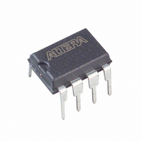
EPC1PC8 Altera, EPC1PC8 Datasheet - Page 7

EPC1PC8
Manufacturer Part Number
EPC1PC8
Description
IC CONFIG DEVICE 1MBIT 8-DIP
Manufacturer
Altera
Series
EPCr
Datasheet
1.EPC1PC8.pdf
(26 pages)
Specifications of EPC1PC8
Programmable Type
OTP
Memory Size
1Mb
Voltage - Supply
3 V ~ 3.6 V, 4.75 V ~ 5.25 V
Operating Temperature
0°C ~ 70°C
Package / Case
8-DIP (0.300", 7.62mm)
For Use With
PLMJ1213 - PROGRAMMER ADAPTER 20 PIN J-LEAD
Lead Free Status / RoHS Status
Contains lead / RoHS non-compliant
Other names
544-1231-5
Available stocks
Company
Part Number
Manufacturer
Quantity
Price
Company:
Part Number:
EPC1PC8
Manufacturer:
INITIO
Quantity:
1 001
Company:
Part Number:
EPC1PC8
Manufacturer:
ALTERA
Quantity:
5 510
Company:
Part Number:
EPC1PC8
Manufacturer:
ALTERA41
Quantity:
5 747
Part Number:
EPC1PC8
Manufacturer:
ALTERA/阿尔特拉
Quantity:
20 000
Company:
Part Number:
EPC1PC8N
Manufacturer:
ALTERA
Quantity:
410
Part Number:
EPC1PC8N
Manufacturer:
ALTERA
Quantity:
20 000
Chapter 4: Configuration Devices for SRAM-Based LUT Devices Data Sheet
Device Configuration
© December 2009
f
1
Altera Corporation
FPGA will reset the device. When the JTAG state machine exits this state,
nINIT_CONF is released and pulled high by an internal 1-k resistor, which in turn
pulls nCONFIG high to begin configuration. If its functionality is not used, the
nINIT_CONF pin does not need to be connected and nCONFIG of the FPGA must be
pulled to V
The EPC2 device’s OE and nCS pins have internal programmable pull-up resistors. If
internal pull-up resistors are used, external pull-up resistors should not be used on
these pins. The internal pull-up resistors are used by default in the Quartus II
software. To turn off the internal pull-up resistors, check the Disable nCS and OE
pull-ups on configuration device option when generating programming files.
The configuration device’s OE and nCS pins control the tri-state buffer on its DATA
output pin, and enable the address counter and oscillator. When OE is driven low, the
configuration device resets the address counter and tri-states its DATA pin. The nCS
pin controls the DATA output of the configuration device. If nCS is held high after the
OE reset pulse, the counter is disabled and the DATA output pin is tri-stated. If nCS is
driven low after the OE reset pulse, the counter and DATA output pin are enabled.
When OE is driven low again, the address counter is reset and the DATA output pin is
tri-stated, regardless of the state of nCS.
If the FPGA’s configuration data exceeds the capacity of a single EPC1 or EPC2
configuration device, multiple EPC1 or EPC2 devices can be cascaded together. If
multiple EPC1 or EPC2 devices are required, the nCASC and nCS pins provide
handshaking between the configuration devices.
EPC1441 and EPC1064/V devices cannot be cascaded.
When configuring ACEX 1K, APEX 20K, APEX II, Arria GX, Cyclone, Cyclone II,
FLEX 10K, Mercury, Stratix, Stratix GX, Stratix II, and Stratix II GX devices with
cascaded EPC1 or EPC2 devices, the position of the EPC1 or EPC2 device in the chain
determines its mode of operation. The first configuration device in the chain is the
master, while subsequent configuration devices are slaves. The nINIT_CONF pin of
the master EPC2 device can be connected to the nCONFIG of the FPGAs, which allows
the INIT_CONF JTAG instruction to begin FPGA configuration. The nCS pin of the
master configuration device is connected to the CONF_DONE of the FPGAs, while its
nCASC pin is connected to nCS of the next slave configuration device in the chain.
Additional EPC1 or EPC2 devices can be chained together by connecting nCASC to
nCS of the next slave EPC1 or EPC2 device in the chain. The last device’s nCS input
comes from the previous device, while its nCASC pin is left floating. All other
configuration pins (DCLK, DATA, and OE) are connected to every device in the chain.
Figure 4–3
configuration device chain and the Altera FPGA.
For specific details about configuration interface connections, including pull-up
resistor values, supply voltages and MSEL pin setting, refer to the appropriate FPGA
family chapter in the
shows the basic configuration interface connections between a
CC
either directly or through a resistor.
Configuration
Handbook.
Configuration Handbook (Complete Two-Volume Set)
4–7


