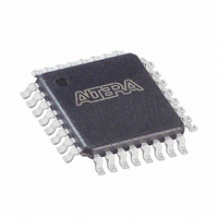
EPC2TI32N Altera, EPC2TI32N Datasheet - Page 14

EPC2TI32N
Manufacturer Part Number
EPC2TI32N
Description
IC CONFIG DEVICE 1.6MBIT 32-TQFP
Manufacturer
Altera
Series
EPCr
Datasheet
1.EPC1PC8.pdf
(26 pages)
Specifications of EPC2TI32N
Programmable Type
In System Programmable
Memory Size
1.6Mb
Voltage - Supply
3 V ~ 3.6 V, 4.5 V ~ 5.5 V
Operating Temperature
-40°C ~ 85°C
Package / Case
32-TQFP, 32-VQFP
Lead Free Status / RoHS Status
Lead free / RoHS Compliant
Other names
544-1648
Available stocks
Company
Part Number
Manufacturer
Quantity
Price
Company:
Part Number:
EPC2TI32N
Manufacturer:
ON
Quantity:
36 000
Company:
Part Number:
EPC2TI32N
Manufacturer:
ALTERA31
Quantity:
2 439
Part Number:
EPC2TI32N
Manufacturer:
ALTERA/阿尔特拉
Quantity:
20 000
4–14 Chapter 4: Configuration Devices for SRAM-Based LUT Devices Data Sheet
IEEE Std. 1149.1 (JTAG) Boundary-Scan Testing
Table 4–6. EPC2 JTAG Instructions
Configuration Handbook (Complete Two-Volume Set)
SAMPLE/PRELOAD
EXTEST
BYPASS
IDCODE
USERCODE
INIT_CONF
ISP Instructions
JTAG Instruction
f
The EPC2 provides JTAG BST circuitry that complies with the IEEE Std. 1149.1-1990
specification. JTAG boundary-scan testing can be performed before or after
configuration, but not during configuration. The EPC2 device supports the JTAG
instructions shown in
For more information, refer to
Testing in Altera Devices)
00 0101 0101
00 0000 0000
11 1111 1111
00 0101 1001
00 0111 1001
00 0110 0001
OPCODE
—
Table
or the EPC2 BSDL files on the Altera web site.
Allows a snapshot of a signal at the device pins to be captured and
examined during normal device operation, and permits an initial data
pattern output at the device pins.
Allows the external circuitry and board-level interconnections to be
tested by forcing a test pattern at the output pins and capturing
results at the input pins.
Places the 1-bit bypass register between the TDI and TDO pins,
which allows the BST data to pass synchronously through a selected
device to adjacent devices during normal device operation.
Selects the device IDCODE register and places it between TDI and
TDO, allowing the device IDCODE to be serially shifted out of TDO.
The device IDCODE for the EPC2 configuration device is shown
below:
0000 0001000000000010 00001101110 1
Selects the USERCODE register and places it between TDI and
TDO, allowing the USERCODE to be serially shifted out of TDO. The
32-bit USERCODE is a programmable user-defined pattern.
This function initiates the FPGA re-configuration process by pulsing
the nINIT_CONF pin low, which is connected to the FPGAs
nCONFIG pins. After this instruction is updated, the nINIT_CONF
pin is pulsed low when the JTAG state machine enters the Run-
Test/Idle state. The nINIT_CONF pin is then released and
nCONFIG is pulled high by the resistor after the JTAG state machine
goes out of Run-Test/Idle state. The FPGA configuration starts after
nCONFIG goes high. As a result, the FPGA is configured with the
new configuration data stored in the configuration device. This
function can be added to your programming file (
the Quartus II software by enabling the Initiate configuration after
programming option in the Programmer options window (Options
menu). This instruction is also used by the MAX+PLUS II software,
.jam files, and .jbc files.
These instructions are used when programming an EPC2 device via
JTAG ports with a USB Blaster, MasterBlaster, ByteBlaster II,
EthernetBlaster, or ByteBlaster MV download cable, or using a .jam,
.jbc, or .svf via an embedded processor.
4–6.
Application Note 39 (IEEE 1149.1 (JTAG) Boundary-Scan
Description
IEEE Std. 1149.1 (JTAG) Boundary-Scan Testing
© December 2009
.pof , .jam, .jbc) in
Altera Corporation


