EPC2TI32N Altera, EPC2TI32N Datasheet - Page 22
EPC2TI32N
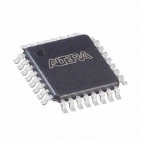
Manufacturer Part Number
EPC2TI32N
Description
IC CONFIG DEVICE 1.6MBIT 32-TQFP
Manufacturer
Altera
Series
EPCr
Datasheet
1.EPC1PC8.pdf
(26 pages)
Specifications of EPC2TI32N
Programmable Type
In System Programmable
Memory Size
1.6Mb
Voltage - Supply
3 V ~ 3.6 V, 4.5 V ~ 5.5 V
Operating Temperature
-40°C ~ 85°C
Package / Case
32-TQFP, 32-VQFP
Lead Free Status / RoHS Status
Lead free / RoHS Compliant
Other names
544-1648
Available stocks
Company
Part Number
Manufacturer
Quantity
Price
Company:

Part Number:
EPC2TI32N
Manufacturer:
ON
Quantity:
36 000
Company:
Part Number:
EPC2TI32N
Manufacturer:
ALTERA31
Quantity:
2 439
Part Number:
EPC2TI32N
Manufacturer:
ALTERA/阿尔特拉
Quantity:
20 000


4–22 Chapter 4: Configuration Devices for SRAM-Based LUT Devices Data Sheet
Table 4–20. EPC1, EPC2 and EPC1441 Pin Functions During Configuration (Part 2 of 3)
Configuration Handbook (Complete Two-Volume Set)
nCS
nCASC
nINIT_CONF
TDI
TDO
Pin Name
PDIP
8-Pin
N/A
N/A
N/A
4
6
(1)
Pin Number
20-Pin
PLCC
12
13
11
9
1
TQFP
32-Pin
10
15
16
13
28
(2)
Input
Output
Open-Drain
Output
Input
Output
Pin Type
Chip select input (active low). The nCS pin connects
to the CONF_DONE of the FPGA.
A low input allows DCLK to increment the address
counter and enables DATA to drive out. If the EPC1
or EPC2 is reset (OE pulled low) while nCS is low,
the device initializes as the master device in a
configuration chain. If the EPC1 or EPC2 device is
reset (OE pulled low) while nCS is high, the device
initializes as a slave device in the chain.
The nCS pin has an internal programmable 1-k
resistor in EPC2 devices. If internal pull-up resistors
are use, external pull-up resistors should not be used
on these pins.The internal pull-up resistors can be
disabled through the Disable nCS and OE pull-ups
on configuration device option.
Cascade select output (active low).
This output goes low when the address counter has
reached its maximum value. When the address
counter has reached its maximum value, the
configuration device has sent all its configuration
data to the FPGA. In a chain of EPC1 or EPC2 devices,
the nCASC pin of one device is connected to the nCS
pin of the next device, which permits DCLK to clock
data from the next EPC1 or EPC2 device in the chain.
For single EPC1 or EPC2 devices and the last device
in the chain, nCASC is left floating.
This pin is only available in EPC1 and EPC2 devices,
which support data cascading.
Allows the INIT_CONF JTAG instruction to initiate
configuration. The nINIT_CONF pin connects to the
nCONFIG of the FPGA.
If multiple EPC2 devices are used to configure a
FPGA, the nINIT_CONF of the first EPC2 pin is tied
to the FPGA’s nCONFIG pin, while subsequent
devices' nINIT_CONF pins are left floating.
The INIT_CONF pin has an internal 1-k pull-up
resistor that is always active in EPC2 devices.
This pin is only available in EPC2 devices.
JTAG data input pin. Connect this pin to V
JTAG circuitry is not used.
This pin is only available in EPC2 devices.
JTAG data output pin. Do not connect this pin if the
JTAG circuitry is not used.
This pin is only available in EPC2 devices.
© December 2009
Description
Altera Corporation
Pin Information
CC
if the
Related parts for EPC2TI32N
Image
Part Number
Description
Manufacturer
Datasheet
Request
R

Part Number:
Description:
IC CONFIG DEVICE 1MBIT 8-DIP
Manufacturer:
Altera
Datasheet:

Part Number:
Description:
IC CONFIG DEVICE 1.6MBIT 20-PLCC
Manufacturer:
Altera
Datasheet:
Part Number:
Description:
IC CONFIG DEVICE 1.6MBIT 20-PLCC
Manufacturer:
Altera
Datasheet:

Part Number:
Description:
IC CONFIG DEVICE 1.6MBIT 32-TQFP
Manufacturer:
Altera
Datasheet:
Part Number:
Description:
IC CONFIG DEVICE 1.6MBIT 32-TQFP
Manufacturer:
Altera
Datasheet:
Part Number:
Description:
IC CONFIG DEVICE 1.6MBIT 20-PLCC
Manufacturer:
Altera
Datasheet:
Part Number:
Description:
IC CONFIG DEVICE 1.6MBIT 20-PLCC
Manufacturer:
Altera
Datasheet:

Part Number:
Description:
IC CONFIG DEVICE 8MBIT 100-PQFP
Manufacturer:
Altera
Datasheet:
Part Number:
Description:
IC CONFIG DEVICE 1.6MBIT 32-TQFP
Manufacturer:
Altera
Datasheet:
Part Number:
Description:
IC CONFIG DEVICE 16MBIT 100-PQFP
Manufacturer:
Altera
Datasheet:
Part Number:
Description:
IC CONFIG DEVICE 16MBIT 100-PQFP
Manufacturer:
Altera
Datasheet:
Part Number:
Description:
IC CONFIG DEVICE 16MBIT 100-PQFP
Manufacturer:
Altera
Datasheet:

Part Number:
Description:
IC CONFIG DEVICE 16MBIT 88-UBGA
Manufacturer:
Altera
Datasheet:
Part Number:
Description:
IC CONFIG DEVICE 212KBIT 20-PLCC
Manufacturer:
Altera
Datasheet:
Part Number:
Description:
IC CONFIG DEVICE 4MBIT 100-PQFP
Manufacturer:
Altera
Datasheet: