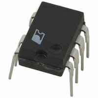
LNK501PN Power Integrations, LNK501PN Datasheet - Page 10

LNK501PN
Manufacturer Part Number
LNK501PN
Description
IC SWIT OCP CV/CC HV 8DIP
Manufacturer
Power Integrations
Series
LinkSwitch®r
Datasheet
1.LNK501PN.pdf
(20 pages)
Specifications of LNK501PN
Output Isolation
Isolated
Frequency Range
26 ~ 46kHz
Voltage - Output
700V
Power (watts)
4W
Operating Temperature
-40°C ~ 150°C
Package / Case
8-DIP (0.300", 7.62mm), 7 Leads
Output Voltage
5.6 V
Input / Supply Voltage (max)
265 VAC
Input / Supply Voltage (min)
85 VAC
Duty Cycle (max)
80 %
Switching Frequency
42 KHz
Supply Current
1.06 mA
Operating Temperature Range
- 40 C to + 150 C
Mounting Style
Through Hole
For Use With
596-1001 - KIT DESIGN ACCELERATOR ADAPTER
Lead Free Status / RoHS Status
Lead free / RoHS Compliant
Other names
596-1031-5
Available stocks
Company
Part Number
Manufacturer
Quantity
Price
Company:
Part Number:
LNK501PN
Manufacturer:
PowerInt
Quantity:
5 700
Part Number:
LNK501PN
Manufacturer:
POWER
Quantity:
20 000
Part Number:
LNK501PN/GN
Manufacturer:
专营POWER
Quantity:
20 000
3. Thermal check – At peak output power, minimum input
Figure 11. Recommended Circuit Board Layout for LinkSwitch using P Package.
10
200 ns to prevent premature termination of the on-cycle.
Verify that the leading edge current spike event is below
current limit at the end of the 200 ns blanking period.
voltage and maximum ambient temperature, verify that the
temperature specifications are not exceeded for LinkSwitch,
transformer, output diode and output capacitors. Enough
thermal margin should be allowed for part-to-part variation of
the R
low line, peak power, a maximum LinkSwitch SOURCE pin
temperature of 100 °C is recommended to allow for these
variations.
LNK501
I
2/05
DS(ON)
Capacitor
Output
of LinkSwitch as specified in the data sheet. Under
Transformer
Capacitor
Y1-
DC Out
-
+
C
S
LinkSwitch
S
S
4. Centered output characteristic – Using a transformer with
nominal primary inductance and at an input voltage midway
between low and high line, verify that the peak power point
occurs at the desired nominal output current, with the correct
output voltage. If this does not occur then the design should
be refined to ensure the overall tolerance limits are met.
Design Tools
Up to date information on design tools can be found at the
Power Integrations website: www.powerint.com.
S
D
S
Input Filter
Capacitor
PI-2900-070202
HV DC
+
-
Input


