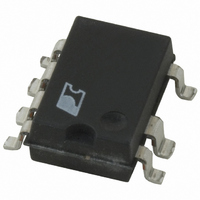
TOP258GN-TL Power Integrations, TOP258GN-TL Datasheet - Page 37

TOP258GN-TL
Manufacturer Part Number
TOP258GN-TL
Description
IC OFFLINE SWIT PROG OVP 8SMD
Manufacturer
Power Integrations
Series
TOPSwitch®-HXr
Type
Off Line Switcherr
Datasheet
1.TOP252GN-TL.pdf
(48 pages)
Specifications of TOP258GN-TL
Output Isolation
Isolated
Frequency Range
119 ~ 145kHz
Voltage - Output
700V
Power (watts)
77W
Operating Temperature
-40°C ~ 150°C
Package / Case
8-SMD Gull Wing, 7 Leads
Output Voltage
700 V
Input / Supply Voltage (max)
9 V
Input / Supply Voltage (min)
- 0.3 V
Duty Cycle (max)
78 %
Switching Frequency
132 KHz
Operating Temperature Range
- 40 C to + 150 C
Mounting Style
SMD/SMT
Maximum Operating Temperature
+ 150 C
Minimum Operating Temperature
- 40 C
Output Current
6.88 A
Output Power
48 W
For Use With
596-1193 - KIT REF DESIGN TOP HX FOR TOP258
Lead Free Status / RoHS Status
Lead free / RoHS Compliant
Other names
596-1190-2
Available stocks
Company
Part Number
Manufacturer
Quantity
Price
Part Number:
TOP258GN-TL
Manufacturer:
POWER
Quantity:
20 000
NOTES:
A.
B.
C.
D.
E.
F.
www.powerint.com
Output (cont.)
ON-State
Resistance
DRAIN Supply Voltage
OFF-State Drain
Leakage Current
Breakdown
Voltage
Rise Time
Fall Time
Supply Voltage Characteristics
Control Supply/
Discharge Current
For specifi cations with negative values, a negative temperature coeffi cient corresponds to an increase in
magnitude with increasing temperature, and a positive temperature coeffi cient corresponds to a decrease in
magnitude with increasing temperature.
Guaranteed by characterization. Not tested in production.
For externally adjusted current limit values, please refer to Figures 55a and 55b (Current Limit vs. External Current Limit Resis-
tance) in the Typical Performance Characteristics section. The tolerance specifi ed is only valid at full current limit.
I
/ F pin connection. See f
The TOPSwitch-HX will start up at 18 V
tures below 0 °C. For reliable start up at 18 V in sub zero temperatures, designers must ensure that circuit capacitors meet
recommended capacitance values.
Breakdown voltage may be checked against minimum BV
exceeding minimum BV
2
f calculation is based on typical values of I
Parameter
DSS
OSC
Symbol
.
R
BV
specifi cation for detail.
I
I
I
DS(ON)
DSS
CD1
CD2
t
t
R
F
DSS
V
DC
MOSFET
X
Enabled
, V
Output
SOURCE = 0 V; T
drain voltage. The capacitance of electrolytic capacitors drops signifi cantly at tempera-
0 V
I
I
I
I
LIMIT
D
D
D
D
V
(Unless Otherwise Specifi ed)
, V
TOP259
TOP260
TOP261
TOP262
= 600 mA
= 700 mA
= 800 mA
= 900 mA
Measured in a Typical Flyback
V
V
M
and f
Output MOSFET Disabled
V
V
V
=
, V
, V
T
DS
Converter Application
J
M
M
OSC,
≤ 85 °C, See Note E
= 560 V, T
Operation
Operation
132 kHz
V
= Floating, I
= Floating, I
66 kHz
Conditions
X
See Note F
, V
i.e. I
T
J
V
= 25 °C
DSS
, V
LIMIT(TYP)
J
M
specifi cation by ramping the DRAIN pin voltage up to but not
J
= -40 to 125 °C
= 0 V
= 125 °C
C
C
2
T
T
T
T
= 4 mA,
= 4 mA,
× f
TOP252-255
TOP256-258
TOP259-262
TOP252-255
TOP256-258
TOP259-262
T
T
T
T
J
J
J
J
J
J
J
J
= 100 °C
= 100 °C
= 100 °C
= 100 °C
OSC
= 25 °C
= 25 °C
= 25 °C
= 25 °C
, where f
OSC
= 66 kHz or 132 kHz depending on package
Min
700
0.6
0.9
1.1
0.8
1.1
1.5
0.3
18
36
1.45
2.25
1.20
1.80
1.05
1.55
0.90
1.35
Typ
100
1.2
1.4
1.6
1.3
1.6
2.2
0.6
TOP252-262
50
Max
1.70
2.60
1.40
2.10
1.20
1.80
1.05
1.55
470
2.0
2.3
2.5
2.2
2.5
2.9
1.3
Units
Rev. F 01/09
mA
μA
ns
ns
Ω
V
V
37


