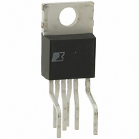
TOP258YN Power Integrations, TOP258YN Datasheet - Page 7
TOP258YN
Manufacturer Part Number
TOP258YN
Description
IC OFFLINE SWIT PROG OVP TO220
Manufacturer
Power Integrations
Series
TOPSwitch®-HXr
Type
Off Line Switcherr
Datasheet
1.TOP252GN-TL.pdf
(48 pages)
Specifications of TOP258YN
Output Isolation
Isolated
Frequency Range
119 ~ 145kHz
Voltage - Output
700V
Power (watts)
195W
Operating Temperature
-40°C ~ 150°C
Package / Case
TO-220-7 (Formed Leads), 5 Leads
Output Voltage
700 V
Input / Supply Voltage (max)
9 V
Input / Supply Voltage (min)
- 0.3 V
Duty Cycle (max)
78 %
Switching Frequency
132 KHz
Operating Temperature Range
- 40 C to + 150 C
Mounting Style
Through Hole
Maximum Operating Temperature
+ 150 C
Minimum Operating Temperature
- 40 C
Output Current
6.88 A
Output Power
195 W
For Use With
596-1193 - KIT REF DESIGN TOP HX FOR TOP258
Lead Free Status / RoHS Status
Lead free / RoHS Compliant
Other names
596-1192-5
Available stocks
Company
Part Number
Manufacturer
Quantity
Price
Company:

Part Number:
TOP258YN
Manufacturer:
SIGE
Quantity:
201
Part Number:
TOP258YN
Manufacturer:
POWER
Quantity:
20 000


Figure 8.
reduction, output overvoltage protection (OVP), external current
limit adjustment, remote ON/OFF and device reset. A
connection to SOURCE pin disables all functions on this pin
and makes TOPSwitch-HX operate in simple three terminal
mode (like TOPSwitch-II).
FREQUENCY (F) Pin (TOP254-258Y, and all E and L packages):
Input pin for selecting switching frequency 132 kHz if connected
to SOURCE pin and 66 kHz if connected to CONTROL pin.
The switching frequency is internally set for fi xed 66 kHz
operation in the P, G, M package and TOP259YN, TOP260YN
and TOP261YN.
SIGNAL GROUND (G) Pin (TOP259YN, TOP260YN &
TOP261YN only):
Return for C pin capacitor and X pin resistor.
SOURCE (S) Pin:
Output MOSFET source connection for high voltage power
return. Primary side control circuit common and reference point.
TOPSwitch-HX Family Functional Description
Like TOPSwitch-GX, TOPSwitch-HX is an integrated switched
mode power supply chip that converts a current at the control
input to a duty cycle at the open drain output of a high voltage
power MOSFET. During normal operation the duty cycle of the
power MOSFET decreases linearly with increasing CONTROL
pin current as shown in Figure 9.
In addition to the three terminal TOPSwitch features, such as
the high voltage start-up, the cycle-by-cycle current limiting,
loop compensation circuitry, auto-restart and thermal
shutdown, the TOPSwitch-HX incorporates many additional
functions that reduce system cost, increase power supply
performance and design fl exibility. A patented high voltage
CMOS technology allows both the high-voltage power MOSFET
and all the low voltage control circuitry to be cost effectively
integrated onto a single monolithic chip.
Three terminals, FREQUENCY, VOLTAGE-MONITOR, and
EXTERNAL CURRENT LIMIT (available in Y and E/L packages),
www.powerint.com
Voltage
Input
P/G Package Externally Set Current Limit.
DC
+
-
R
IL
D
S
CONTROL
M
C
For R
For R
See Figure 55b for other
resistor values (R
select different I
I
I
LIMIT
LIMIT
IL
IL
= 61%
= 37%
= 12 k
= 19 k
PI-4713-021308
LIMIT
IL
) to
values.
two terminals, VOLTAGE-MONITOR and EXTERNAL CURRENT
LIMIT (available in M package) or one terminal MULTI-FUNCTION
(available in P and G package) have been used to implement
some of the new functions. These terminals can be connected
to the SOURCE pin to operate the TOPSwitch-HX in a
TOPSwitch-like three terminal mode. However, even in this three
terminal mode, the TOPSwitch-HX offers many transparent
features that do not require any external components:
1.
2.
3.
Figure 9.
A fully integrated 17 ms soft-start signifi cantly reduces or
eliminates output overshoot in most applications by sweeping
both current limit and frequency from low to high to limit the
peak currents and voltages during start-up.
A maximum duty cycle (DC
storage capacitor, lower input voltage requirement and/or
higher power capability.
Multi-mode operation optimizes and improves the power
supply effi ciency over the entire load range while maintaining
good cross regulation in multi-output supplies.
100
132
78
55
25
66
30
Control Pin Characteristics (Multi-Mode Operation).
I
CD1
Full Frequency Mode
Auto-Restart
I
B
Jitter
I
C01
MAX
(constant over load range)
) of 78% allows smaller input
TOP252-262
Slope = PWM Gain
Frequency
Variable
I
Mode
C02
I
C03
I
COFF
Frequency
PI-4645-041107
Multi-Cycle
Modulation
CONTROL
CONTROL
Mode
Low
CONTROL
Current
Current
Current
Rev. F 01/09
7
Related parts for TOP258YN
Image
Part Number
Description
Manufacturer
Datasheet
Request
R

Part Number:
Description:
SOP-16
Manufacturer:
Power Integrations
Datasheet:
Part Number:
Description:
DIP8
Manufacturer:
Power Integrations
Datasheet:
Part Number:
Description:
TO-263
Manufacturer:
Power Integrations
Datasheet:
Part Number:
Description:
TO-263
Manufacturer:
Power Integrations
Datasheet:
Part Number:
Description:
Manufacturer:
Power Integrations
Datasheet: