TOP246YN Power Integrations, TOP246YN Datasheet - Page 20
TOP246YN
Manufacturer Part Number
TOP246YN
Description
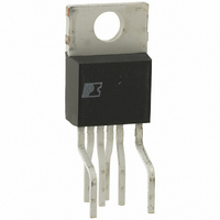
IC OFFLINE SWIT UVLO HV TO220
Manufacturer
Power Integrations
Series
TOPSwitch®-GXr
Type
Off Line Switcherr
Datasheet
1.TOP242GN-TL.pdf
(52 pages)
Specifications of TOP246YN
Output Isolation
Isolated
Frequency Range
66 ~ 132kHz
Voltage - Output
700V
Power (watts)
125W
Operating Temperature
-40°C ~ 150°C
Package / Case
TO-220-7 (Formed Leads), 5 Leads
Output Voltage
12 V
Input / Supply Voltage (max)
265 VAC
Input / Supply Voltage (min)
85 VAC
Duty Cycle (max)
83 %
Switching Frequency
132 KHz
Supply Current
2.2 mA
Operating Temperature Range
- 40 C to + 150 C
Mounting Style
Through Hole
No. Of Outputs
1
Output Current
4.32A
No. Of Pins
6
Rohs Compliant
Yes
Lead Free Status / RoHS Status
Lead free / RoHS Compliant
Other names
596-1077-5
Available stocks
Company
Part Number
Manufacturer
Quantity
Price
Company:

Part Number:
TOP246YN
Manufacturer:
POWER
Quantity:
4 000
Company:
Part Number:
TOP246YN
Manufacturer:
POWER
Quantity:
10 000
Part Number:
TOP246YN
Manufacturer:
POWER
Quantity:
20 000


Figure 41. 30 W Power Supply using External Current Limit Programming and Line Sensing for UV and OV.
Application Examples
A High Efficiency, 30 W, Universal Input Power Supply
The circuit shown in Figure 41 takes advantage of several of
the TOPSwitch-GX features to reduce system cost and power
supply size and to improve efficiency. This design delivers
30 W at 12 V, from an 85 VAC to 265 VAC input, at an ambient
of 50 °C, in an open frame configuration. A nominal efficiency
of 80% at full load is achieved using TOP244Y.
The current limit is externally set by resistors R1 and R2 to a
value just above the low line operating peak DRAIN current
of approximately 70% of the default current limit. This
allows use of a smaller transformer core size and/or higher
transformer primary inductance for a given output power,
reducing TOPSwitch-GX power dissipation, while at the same
time avoiding transformer core saturation during startup and
output transient conditions. The resistors R1 & R2 provide a
signal that reduces the current limit with increasing line voltage,
which in turn limits the maximum overload power at high input
line voltage. This function in combination with the built-in
soft-start feature of TOPSwitch-GX, allows the use of a low cost
RCD clamp (R3, C3 and D1) with a higher reflected voltage,
by safely limiting the TOPSwitch-GX drain voltage, with
adequate margin under worst case conditions. Resistor R4
provides line sensing, setting UV at 100 VDC and OV at
450 VDC. The extended maximum duty cycle feature of
PERFORMANCE SUMMARY
Output Power:
Regulation:
Efficiency:
Ripple:
250 VAC
20
100 nF
CX1
TOP242-250
J1
N
L
20 mH
L1
O
11/05
3.15 A
F1
600 V
BR1
2A
30 W
± 4%
≥ 79%
≤ 50 mV pk-pk
68 µF
400 V
C1
4.7 nF
1 kV
4.7 MΩ
9.09 kΩ
1/2 W
C3
1/2 W
2 MΩ
R1
R2
UF4005
R4
D1
D
S
68 kΩ
2 W
CONTROL
CONTROL
R3
X
L
F
2.2 nF
CY1
C
TOPSwitch-GX
T1
47 µF
10 V
C5
TOP244Y
TOPSwitch-GX (guaranteed minimum value of 75% vs. 64%
for TOPSwitch-II) allows the use of a smaller input capacitor
(C1). The extended maximum duty cycle and the higher
reflected voltage possible with the RCD clamp also permit
the use of a higher primary to secondary turns ratio for T1,
which reduces the peak reverse voltage experienced by the
secondary rectifier D8. As a result a 60 V Schottky rectifier
can be used for up to 15 V outputs, which greatly improves
power supply efficiency. The frequency reduction feature of the
TOPSwitch-GX eliminates the need for any dummy loading
for regulation at no load and reduces the no-load/standby
consumption of the power supply. Frequency jitter provides
improved margin for conducted EMI, meeting the CISPR 22
(FCC B) specification.
Output regulation is achieved by using a simple Zener sense
circuit for low cost. The output voltage is determined by the
Zener diode (VR2) voltage and the voltage drops across the
optocoupler (U2) LED and resistor R6. Resistor R8 provides
bias current to Zener VR2 for typical regulation of ±5% at
the 12 V output level, over line and load and component
variations.
A High Efficiency, Enclosed, 70 W, Universal Adapter Supply
The circuit shown in Figure 42 takes advantage of several of the
TOPSwitch-GX features to reduce cost, power supply size and
6.8 Ω
U1
R5
1 nF
C14
MBR1060
D8
150 Ω
1N4148
R15
D2
0.1 µF
560 µF
35 V
C6
C10
560 µF
35 V
C11
150 Ω
R6
3.3 µH
VR2
1N5240C
10 V, 2%
L3
LTV817A
U2
150 Ω
R8
220 µF
35 V
C12
PI-2657-081204
12 V @
2.5 A
RTN
Related parts for TOP246YN
Image
Part Number
Description
Manufacturer
Datasheet
Request
R

Part Number:
Description:
SOP-16
Manufacturer:
Power Integrations
Datasheet:
Part Number:
Description:
DIP8
Manufacturer:
Power Integrations
Datasheet:
Part Number:
Description:
TO-263
Manufacturer:
Power Integrations
Datasheet:
Part Number:
Description:
TO-263
Manufacturer:
Power Integrations
Datasheet:
Part Number:
Description:
Manufacturer:
Power Integrations
Datasheet: