TOP246FN Power Integrations, TOP246FN Datasheet - Page 38
TOP246FN
Manufacturer Part Number
TOP246FN
Description
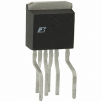
IC OFFLINE SWIT UVLO HV TO262
Manufacturer
Power Integrations
Series
TOPSwitch®-GXr
Type
Off Line Switcherr
Datasheet
1.TOP242GN-TL.pdf
(52 pages)
Specifications of TOP246FN
Output Isolation
Isolated
Frequency Range
66 ~ 132kHz
Voltage - Output
700V
Power (watts)
125W
Operating Temperature
-40°C ~ 150°C
Package / Case
TO-262-7 (Formed Leads), 5 Leads
Output Voltage
12 V
Input / Supply Voltage (max)
265 VAC
Input / Supply Voltage (min)
85 VAC
Duty Cycle (max)
83 %
Switching Frequency
132 KHz
Supply Current
2.2 mA
Operating Temperature Range
- 40 C to + 150 C
Mounting Style
Through Hole
Lead Free Status / RoHS Status
Lead free / RoHS Compliant
Other names
596-1168
TOP246FN
TOP246FN
Available stocks
Company
Part Number
Manufacturer
Quantity
Price

Company:
Part Number:
TOP246FN
Manufacturer:
POWER
Quantity:
3 588
Company:
Part Number:
TOP246FN
Manufacturer:
POWER
Quantity:
15 000
Part Number:
TOP246FN
Manufacturer:
POWER
Quantity:
20 000


NOTES:
A. For specifications with negative values, a negative temperature coefficient corresponds to an increase in
B. Guaranteed by characterization. Not tested in production.
C. For externally adjusted current limit values, please refer to Figures 54b, 55b and 56b (Current Limit vs. External
D. Breakdown voltage may be checked against minimum BV
E. It is possible to start up and operate TOPSwitch-GX at DRAIN voltages well below 36 V. However, the CONTROL
38
OUTPUT (cont.)
ON-State
Resistance
OFF-State Drain
Leakage Current
Breakdown
Voltage
Rise Time
Fall Time
SUPPLY VOLTAGE CHARACTERISTICS
DRAIN Supply
Voltage
Shunt Regulator
Voltage
Shunt Regulator
Temperature Drift
Control Supply/
Discharge Current
magnitude with increasing temperature, and a positive temperature coefficient corresponds to a decrease in
magnitude with increasing temperature.
Current Limit Resistance) in the Typical Performance Characteristics section. The tolerance specified is only valid
at full current limit.
to but not exceeding minimum BV
pin charging current is reduced, which affects start-up time, auto-restart frequency, and auto-restart duty cycle.
Refer to Figure 68, the characteristic graph on CONTROL pin charge current (I
voltage operation characteristics.
TOP242-250
Parameter
O
11/05
Symbol
V
R
BV
C(SHUNT)
I
I
I
DS(ON)
DSS
CD1
CD2
t
t
R
F
DSS
Output MOSFET
V
DSS
X
SOURCE = 0 V; T
I
I
, V
D
D
.
TOP249
TOP250
Enabled
Measured in a Typical Flyback
= 600 mA
= 700 mA
(Unless Otherwise Specified)
L
V
V
, V
V
L
L
See Note D, T
, V
, V
DS
Converter Application
M
= 0 V
M
M
Output MOSFET
= 560 V; T
V
See Figure 53
Conditions
= Floating; I
= Floating; I
X
See Note E
, V
I
Disabled
C
L
= 4 mA
, V
J
M
= -40 to 125 °C
J
TOP242-245
TOP246-249
= 0 V
J
T
T
= 125 °C
T
T
= 25 °C
J
J
TOP250
J
J
C
C
DSS
= 100 °C
= 100 °C
= 25 °C
= 25 °C
= 4 mA
= 4 mA
specification by ramping the DRAIN pin voltage up
Min
5.60
700
1.0
1.2
1.3
0.3
36
C
) vs. DRAIN voltage for low
Typ
1.30
2.15
1.10
1.85
5.85
100
±50
1.6
2.2
2.4
0.6
50
Max
1.50
2.50
1.28
2.15
6.10
3.65
470
2.5
3.2
1.3
ppm/°C
Units
mA
µA
ns
ns
Ω
V
V
V
Related parts for TOP246FN
Image
Part Number
Description
Manufacturer
Datasheet
Request
R

Part Number:
Description:
SOP-16
Manufacturer:
Power Integrations
Datasheet:
Part Number:
Description:
DIP8
Manufacturer:
Power Integrations
Datasheet:
Part Number:
Description:
TO-263
Manufacturer:
Power Integrations
Datasheet:
Part Number:
Description:
TO-263
Manufacturer:
Power Integrations
Datasheet:
Part Number:
Description:
Manufacturer:
Power Integrations
Datasheet: