VIPER100-E STMicroelectronics, VIPER100-E Datasheet - Page 8
VIPER100-E
Manufacturer Part Number
VIPER100-E
Description
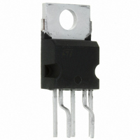
IC SWIT PWM SMPS CM PENTAWATT5
Manufacturer
STMicroelectronics
Series
VIPER™r
Datasheet
1.VIPER100-E.pdf
(29 pages)
Specifications of VIPER100-E
Output Isolation
Isolated
Frequency Range
90 ~ 200kHz
Voltage - Input
8 ~ 15 V
Voltage - Output
620V
Power (watts)
82W
Operating Temperature
25°C ~ 125°C
Package / Case
Pentawatt-5 HV (Bent and Staggered Leads)
Output Voltage
620 V
Output Current
3 A
Input Voltage
0 V to 15 V
Switching Frequency
200 KHz
Operating Temperature Range
- 65 C to + 150 C
Mounting Style
Through Hole
No. Of Pins
5
Ic Generic Number
100
Output Current Max
5.3A
Frequency
200kHz
Leaded Process Compatible
Yes
Output Current Min
3A
Rohs Compliant
Yes
Lead Free Status / RoHS Status
Lead free / RoHS Compliant
Other names
497-6161-5
Available stocks
Company
Part Number
Manufacturer
Quantity
Price
Company:

Part Number:
VIPER100-E
Manufacturer:
ROHM
Quantity:
12 000
Company:
Part Number:
VIPER100-E
Manufacturer:
STMicroelectronics
Quantity:
1 818


3 Pin Description
3
3.1
3.2
3.3
3.4
8/29
Pin Description
Drain Pin (Integrated Power MOSFET Drain):
Integrated Power MOSFET drain pin. It provides internal bias current during start-up via an
integrated high voltage current source which is switched off during normal operation. The
device is able to handle an unclamped current during its normal operation, assuring self
protection against voltage surges, PCB stray inductance, and allowing a snubberless operation
for low output power.
Source Pin:
Power MOSFET source pin. Primary side circuit common ground connection.
V
This pin provides two functions :
Compensation Pin
This pin provides two functions :
DD
It corresponds to the low voltage supply of the control part of the circuit. If V
8V, the start-up current source is activated and the output power MOSFET is switched off
until the V
reduced, the V
ground. After that, the current source is shut down, and the device tries to start up by
switching again.
This pin is also connected to the error amplifier, in order to allow primary as well as
secondary regulation configurations. In case of primary regulation, an internal 13V
trimmed reference voltage is used to maintain V
voltage between 8.5V and 12.5V will be put on V
stuck the output of the transconductance amplifier to the high state. The COMP pin
behaves as a constant current source, and can easily be connected to the output of an
optocoupler. Note that any overvoltage due to regulation loop failure is still detected by the
error amplifier through the V
will be somewhat higher than the nominal one, but still under control.
It is the output of the error transconductance amplifier, and allows for the connection of a
compensation network to provide the desired transfer function of the regulation loop. Its
bandwidth can be easily adjusted to the needed value with usual components value. As
stated above, secondary regulation configurations are also implemented through the
COMP pin.
When the COMP voltage is going below 0.5V, the shut-down of the circuit occurs, with a
zero duty cycle for the power MOSFET. This feature can be used to switch off the
converter, and is automatically activated by the regulation loop (no matter what the
configuration is) to provide a burst mode operation in case of negligible output power or
open load condition.
Pin (Power Supply):
DD
voltage reaches 11V. During this phase, the internal current consumption is
DD
pin is sourcing a current of about 2mA and the COMP pin is shorted to
DD
voltage, which cannot overpass 13V. The output voltage
DD
DD
at 13V. For secondary regulation, a
pin by transformer design, in order to
DD
VIPer100-E
goes below
Related parts for VIPER100-E
Image
Part Number
Description
Manufacturer
Datasheet
Request
R

Part Number:
Description:
STMicroelectronics [RIPPLE-CARRY BINARY COUNTER/DIVIDERS]
Manufacturer:
STMicroelectronics
Datasheet:
Part Number:
Description:
STMicroelectronics [LIQUID-CRYSTAL DISPLAY DRIVERS]
Manufacturer:
STMicroelectronics
Datasheet:

Part Number:
Description:
BOARD EVAL FOR MEMS SENSORS
Manufacturer:
STMicroelectronics
Datasheet:
Part Number:
Description:
NPN TRANSISTOR POWER MODULE
Manufacturer:
STMicroelectronics
Datasheet:
Part Number:
Description:
TURBOSWITCH ULTRA-FAST HIGH VOLTAGE DIODE
Manufacturer:
STMicroelectronics
Datasheet:
Part Number:
Description:
Manufacturer:
STMicroelectronics
Datasheet:
Part Number:
Description:
DIODE / SCR MODULE
Manufacturer:
STMicroelectronics
Datasheet:
Part Number:
Description:
DIODE / SCR MODULE
Manufacturer:
STMicroelectronics
Datasheet:
Part Number:
Description:
Search -----> STE16N100
Manufacturer:
STMicroelectronics
Datasheet:
Part Number:
Description:
Search ---> STE53NA50
Manufacturer:
STMicroelectronics
Datasheet:
Part Number:
Description:
NPN Transistor Power Module
Manufacturer:
STMicroelectronics
Datasheet:
Part Number:
Description:
DIODE / SCR MODULE
Manufacturer:
STMicroelectronics
Datasheet: