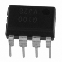
FSQ100 Fairchild Semiconductor, FSQ100 Datasheet

FSQ100
Specifications of FSQ100
Available stocks
Related parts for FSQ100
FSQ100 Summary of contents
Page 1
... FPS™ trademark of Fairchild Semiconductor Corporation. © 2007 Fairchild Semiconductor Corporation FSQ100 Rev. 1.0.2 Description The FSQ100 consists of an integrated Pulse Width Modulator (PWM) and SenseFET, specifically designed for high-performance, off-line, Switch-Mode Power Supplies (SMPS) with minimal external components. This device is an integrated high-voltage power switching regulator that combines a VDMOS SenseFET with a voltage mode PWM control block ...
Page 2
... AC AC Internal Block Diagram UVLO I I delay fb µA 40 0µ Reset Min.20V © 2007 Fairchild Semiconductor Corporation FSQ100 Rev. 1.0.2 V Drain STR PWM V V GND FB CC Figure 1. Typical Flyback Application Open Frame (2) ±15% 230V AC 13W Internal Voltage Bias Ref 9/7V Vck ...
Page 3
... SenseFET Drain. The drain pins are designed to connect directly to the primary lead of the 6,7,8 Drain transformer and are capable of switching a maximum of 650V. Minimizing the length of the trace connecting these pins to the transformer decreases leakage inductance. © 2007 Fairchild Semiconductor Corporation FSQ100 Rev. 1.0.2 Drain GND ...
Page 4
... Junction-to-Case Thermal Impedance JC Notes: 3. Free-standing with no heatsink; without copper clad. Measurement condition; just before junction temperature T enters into OTP. 4. Measured on the DRAIN pin close to plastic interface. © 2007 Fairchild Semiconductor Corporation FSQ100 Rev. 1.0.2 = 25°C, unless otherwise specified. A Parameter Parameter (3) (4) 4 Value ...
Page 5
... Pulse test: Pulse width ≤ 300µs, duty ≤ 2%. 6. These parameters, although guaranteed, are tested in EDS (wafer test) process. 7. These parameters, although guaranteed, are not 100% tested in production. 8. Control part only. © 2007 Fairchild Semiconductor Corporation FSQ100 Rev. 1.0.2 Conditions V =650V ...
Page 6
... Temperature [°C] Figure 6. Start Threshold Voltage (V 1.15 1.10 1.05 1.00 0.95 0.90 0.85 - Temperature [°C] Figure 8. Operating Frequency (f © 2007 Fairchild Semiconductor Corporation FSQ100 Rev. 1.0.2 = 25°C. A 1.15 1.10 1.05 1.00 0.95 0.90 0.85 100 150 -50 ) vs. T Figure 5. OVP A 1.15 1.10 1 ...
Page 7
... Temperature [°C] Figure 10. Peak Current Limit (I 1.15 1.10 1.05 1.00 0.95 0.90 0.85 - Temperature [°C] Figure 12. Shutdown Delay Current (I © 2007 Fairchild Semiconductor Corporation FSQ100 Rev. 1.0.2 (Continued) = 25°C. A 1.15 1.10 1.05 1.00 0.95 0.90 0.85 -50 100 150 ) vs. T Figure 11. LIM A 1 ...
Page 8
... V CC 9V/ 7V Figure 14. Internal Startup Circuit Calculating the V capacitor is an important step to CC design with the FSQ100. At initial startup, the maximum value of start operating current I which supplies current to UVLO and V charging current I of the V VCC CC – 100µA. After V reaches the UVLO start voltage, only ...
Page 9
... LIM ). Burst Operation: To minimize the power dissipation standby mode, the FSQ100 enters burst-mode slowly operation. As the load decreases, the feedback voltage FB decreases. The device automatically enters burst mode when the feedback voltage drops below V At this point, switching stops and the output voltages start to drop ...
Page 10
... F capacitor (C ); and decrease a feedback gain resistor shown in Figure 23. F © 2007 Fairchild Semiconductor Corporation FSQ100 Rev. 1.0.2 the chattering or Figure 22. Figure 23. 2. Reference Materials AN-4134 — Design Guidelines for Off-line Forward Converters using FPS™ AN-4137 — Design Guidelines for Off-line Flyback Converters using FPS™ ...
Page 11
... Physical Dimensions PIN 1 INDICATOR HALF LEAD 4X 0.005 [0.126] MAX 0.210 [5.334] SEATING PLANE MIN 0.015 [0.381] 0.100 [2.540 0.022 0.562 0.014 0.358 0.10 © 2007 Fairchild Semiconductor Corporation FSQ100 Rev. 1.0 0.400 10.160 0.355 9.017 0.280 7.112 0.240 6.096 1 4 FULL LEAD 4X ...
Page 12
... Fairchild Semiconductor Corporation FSQ100 Rev. 1.0.2 12 www.fairchildsemi.com ...


