LNK354PN Power Integrations, LNK354PN Datasheet
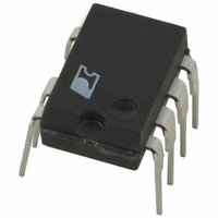
IC OFFLINE SWIT OCP HV 8DIP

LNK354PN

Manufacturer Part Number
LNK354PN
Description
IC OFFLINE SWIT OCP HV 8DIP
Manufacturer
Power Integrations
Series
LinkSwitch®-HFr
Type
Off Line Switcherr
Datasheet

Specifications of LNK354PN

Output Isolation
Isolated
Frequency Range
186 ~ 214kHz
Voltage - Output
700V
Power (watts)
5W
Operating Temperature
-40°C ~ 150°C
Package / Case
8-DIP (0.300", 7.62mm), 7 Leads
Output Voltage
5.8 V
Input / Supply Voltage (max)
265 VAC
Input / Supply Voltage (min)
85 VAC
Duty Cycle (max)
63 %
Switching Frequency
132 KHz
Supply Current
280 uA
Operating Temperature Range
- 40 C to + 150 C
Mounting Style
Through Hole
Lead Free Status / RoHS Status
Lead free / RoHS Compliant

Available stocks

Company
Part Number
Manufacturer
Quantity
Price
Part Number:
LNK354PN
Manufacturer:
power
Quantity:
15 000
Part Number:
LNK354PN
Manufacturer:
POWER
Quantity:
20 000
Part Number:
LNK354PN
Manufacturer:
POWER
Quantity:
10 992
Company:
Part Number:
LNK354PN
Quantity:
18 200
Features Optimized for Lowest System Cost
Much Better Performance over Linear/RCC
EcoSmart
Applications
Description
LinkSwitch-HF integrates a 700 V power MOSFET, oscillator,
simple ON/OFF control scheme, a high voltage switched current
LNK353/354
LinkSwitch-HF Family
Enhanced, Energy Efficient, Low Power
Off-Line Switcher IC
Fully integrated auto-restart for short-circuit and open
loop protection
Self-biased supply – saves transformer auxiliary winding
and associated bias supply components
Tight tolerances and negligible temperature variation on
key parameters eases design and lowers cost
High maximum switching frequency allows very low
flux density transformer designs, practically eliminating
audible noise
Frequency jittering greatly reduces EMI
Packages with large creepage to high voltage pin
Lowest component count switcher solution
Lower system cost than RCC, discrete PWM and other
integrated solutions
Universal input range allows worldwide operation
Simple ON/OFF control – no loop compensation needed
No bias winding – simpler, lower cost transformer
High frequency switching – smaller and lower cost
transformer
Very low component count – higher reliability and single
side printed circuit board
High bandwidth provides fast turn on with no overshoot
and excellent transient load response
Current limit operation rejects line frequency ripple
Built-in current limit and hysteretic thermal shutdown
protection
No-load consumption <300 mW without bias winding at
265 VAC input
Meets California Energy Commission (CEC), Energy
Star, and EU requirements
Chargers for cell/cordless phones, PDAs, digital cameras,
MP3/portable audio devices, shavers etc.
Standby and auxiliary supplies
®
– Extremely Energy Efficient
Product Highlights
®
Table 1. Notes: 1. Typical continuous power in a non-ventilated
enclosed adapter measured at 50 °C ambient. 2. Maximum practical
continuous power in an open frame design with adequate heat
sinking, measured at 50 °C ambient. 3. Packages: P: DIP-8B,
G: SMD-8B. For lead-free package options, see Part Ordering
Information. 4. For designs without a Y capacitor, the available power
may be lower (see Key Applications Considerations).
source, frequency jittering, cycle-by-cycle current limit, and
thermal shutdown circuitry onto a monolithic IC. The start-up
and operating power are derived directly from the DRAIN pin,
eliminating the need for a bias winding and associated circuitry.
The 200 kHz maximum switching frequency allows very
low flux transformer designs, practically eliminating audible
noise with the simple ON/OFF control scheme using standard
varnished transformer construction. Efficient operation at this
high switching frequency is achieved due to the optimized
switching characteristics and small capacitances of the integrated
power MOSFET. The fully integrated auto-restart circuit safely
limits output power during fault conditions such as output short
circuit or open loop, reducing component count and secondary
feedback circuitry cost. The internal oscillator frequency is
jittered to significantly reduce both the quasi-peak and average
EMI, minimizing filtering cost.
Figure 1. Typical Standby Application.
LNK353 P or G
LNK354 P or G
PRODUCT
HV DC Input
+
Wide Range
LinkSwitch-HF
OUTPUT POWER TABLE
(3)
Adapter
230 VAC ±15%
3.5 W
3 W
D
S
(1)
FB
BP
Frame
Open
4 W
5 W
(2)
Adapter
2.5 W
3 W
85-265 VAC
(4)
(4)
February 2005
(1)
Output
PI-3855-022704
DC
Frame
4.5 W
Open
3 W
+
(2)

Related parts for LNK354PN

LNK354PN Summary of contents

Page 1

LNK353/354 LinkSwitch-HF Family Enhanced, Energy Efficient, Low Power Off-Line Switcher IC Product Highlights Features Optimized for Lowest System Cost • Fully integrated auto-restart for short-circuit and open loop protection • Self-biased supply – saves transformer auxiliary winding and associated bias ...

Page 2

LNK353/354 BYPASS (BP) 6.3 V JITTER OSCILLATOR FEEDBACK 1. (FB) Figure 2. Functional Block Diagram. Pin Functional Description DRAIN (D) Pin: Power MOSFET drain connection. Provides internal operating current for both start-up and steady-state operation. BYPASS (BP) ...

Page 3

LinkSwitch-HF Functional Description LinkSwitch-HF combines a high voltage power MOSFET switch with a power supply controller in one device. Unlike conventional PWM (pulse width modulator) controllers, LinkSwitch-HF uses a simple ON/OFF control to regulate the output voltage. The LinkSwitch-HF controller ...

Page 4

LNK353/354 D1 D2 1N4005 1N4005 RF1 8.2 Ω 2 4.7 µF 85-265 VAC 400 1N4005 1N4005 Figure 5. Universal Input, 5.7 V, 400 mA, Constant Voltage, Constant Current Battery Charger ...

Page 5

Key Application Considerations LinkSwitch-HF Design Considerations Output Power Table Data sheet maximum output power table (Table 1) represents the maximum practical continuous output power level that can be obtained under the following assumed conditions: 1. The minimum DC input voltage ...

Page 6

... Under low line, maximum power, does not exceed a maximum LinkSwitch-HF SOURCE pin temperature of DS 100 °C is recommended to allow for these variations. Design Tools Up-to-date information on design tools can be found at the Power Integrations website: www.powerint.com. Input Filter Capacitor Y1- Capacitor m PRI ...

Page 7

DRAIN Voltage .................................. ................ -0 700 V Peak DRAIN Current......................................400 mA (750 mA) FEEDBACK Voltage ................................................ -0 FEEDBACK Current .................................................... 100 mA BYPASS Voltage...................................................... -0 Storage Temperature .......................................... -65 °C ...

Page 8

LNK353/354 Parameter Symbol CONTROL FUNCTIONS (cont) BYPASS Pin I Supply Current BPSC CIRCUIT PROTECTION I LIMIT Current Limit (See Note E) Minimum On Time t ON(MIN) Leading Edge t Blanking Time LEB Thermal Shutdown T SD Temperature Thermal Shutdown T ...

Page 9

Parameter Symbol OUTPUT (cont) DRAIN Supply Voltage Output Enable t Delay EN Output Disable t Setup Time DST Auto-Restart t ON-Time AR Auto-Restart Duty DC Cycle AR NOTES: A. Total current consumption is the sum of I switching) and the ...

Page 10

LNK353/354 Figure 7. LinkSwitch-HF General Test Circuit 90% DRAIN VOLTAGE 10 Figure 8. LinkSwitch-HF Duty Cycle Measurement 2/05 470 Ω ...

Page 11

Typical Performance Characteristics 1.1 1.0 0.9 -50 - 100 125 150 Junction Temperature (°C) Figure 10. Breakdown vs. Temperature. 1.4 1.2 1.0 0.8 Normalized di/dt 0.6 0.4 0 Temperature (°C) Figure 12. ...

Page 12

LNK353/354 Typical Performance Characteristics (cont.) PART ORDERING INFORMATION LNK 354 2/05 1000 100 100 200 300 400 500 Drain Voltage (V) Figure 16. C vs. Drain Voltage. OSS LinkSwitch Product Family ...

Page 13

D S .004 (.10) -E- .240 (6.10) .260 (6.60) Pin 1 .367 (9.32) -D- .387 (9.83) .125 (3.18) .145 (3.68) -T- SEATING PLANE .100 (2.54) BSC .048 (1.22) .053 (1.35) .014 (.36) ⊕ .010 (.25) ...

Page 14

LNK353/354 14 F 2/05 Notes ...

Page 15

Notes LNK353/354 15 F 2/05 ...

Page 16

... For the latest updates, visit our website: www.powerint.com Power Integrations reserves the right to make changes to its products at any time to improve reliability or manufacturability. Power Integrations does not assume any liability arising from the use of any device or circuit described herein. POWER INTEGRATIONS MAKES NO WARRANTY HEREIN AND SPECIFICALLY DISCLAIMS ALL WARRANTIES INCLUDING, WITHOUT LIMITATION, THE IMPLIED WARRANTIES OF MERCHANTABILITY, FITNESS FOR A PARTICULAR PURPOSE, AND NON-INFRINGEMENT OF THIRD PARTY RIGHTS ...

Related keywords