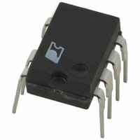
LNK364PN Power Integrations, LNK364PN Datasheet - Page 4

LNK364PN
Manufacturer Part Number
LNK364PN
Description
IC OFFLINE SWIT HV 8DIP
Manufacturer
Power Integrations
Series
LinkSwitch®-XTr
Type
Off Line Switcherr
Datasheet
1.LNK362PG.pdf
(16 pages)
Specifications of LNK364PN
Output Isolation
Isolated
Frequency Range
124 ~ 140kHz
Voltage - Output
700V
Power (watts)
9W
Operating Temperature
-40°C ~ 150°C
Package / Case
8-DIP (0.300", 7.62mm), 7 Leads
Output Voltage
5.8 V
Input / Supply Voltage (max)
265 VAC
Input / Supply Voltage (min)
85 VAC
Duty Cycle (max)
60 %
Switching Frequency
132 KHz
Supply Current
250 uA
Operating Temperature Range
- 40 C to + 150 C
Mounting Style
Through Hole
For Use With
596-1105 - DESIGN ACCELERATOR KIT XT SWITCH
Lead Free Status / RoHS Status
Lead free / RoHS Compliant
Other names
596-1088-2
596-1088-2
596-1088-5
596-1088-2
596-1088-5
Available stocks
Company
Part Number
Manufacturer
Quantity
Price
Company:
Part Number:
LNK364PN
Manufacturer:
PowerInt
Quantity:
2 300
Part Number:
LNK364PN
Manufacturer:
POWER
Quantity:
20 000
Figure 5. 2 W Universal Input CV Adapter Using LNK362.
Applications Example
A 2 W CV Adapter
The schematic shown in Figure 5 is a typical implementation of
a universal input, 6.2 V ±7%, 322 mA adapter using LNK362.
This circuit makes use of the Clampless technique to eliminate the
primary clamp components and reduce the cost and complexity
of the circuit.
The EcoSmart features built into the LinkSwitch-XT family
allow this design to easily meet all current and proposed
energy effi ciency standards, including the mandatory California
Energy Commission (CEC) requirement for average operating
effi ciency.
The AC input is rectifi ed by D1 to D4 and fi ltered by the bulk
storage capacitors C1 and C2. Resistor RF1 is a fl ameproof,
fusible, wire wound type and functions as a fuse, inrush current
limiter and, together with the π fi lter formed by C1, C2, L1
and L2, differential mode noise attenuator. Resistor R1 damps
ringing caused by L1 and L2.
This simple input stage, together with the frequency jittering of
LinkSwitch-XT, a low value Y1 capacitor and PI’s E-Shield™
windings within T1, allow the design to meet both conducted
and radiated EMI limits with >10 dBμV margin. The low value
of CY1 is important to meet the requirement for a very low
touch current (the line frequency current that fl ows through
CY1) often specifi ed for adapters, in this case <10 μA.
Rev. E 11/08
2-4
4
4
J1
85-265
J2
VRMS
LNK362-364
2.5 W
8.2 Ω
RF1
1N4005
1N4005
D1
D3
1N4005
1N4005
3.3 μF
400 V
D2
D4
C1
1/8 W
1 mH
1 mH
3.9 k
R1
L1
L2
LinkSwitch-XT
3.3 μF
400 V
C2
LNK362P
U1
4
5
3
The rectifi ed and fi ltered input voltage is applied to the primary
winding of T1. The other side of the primary is driven by the
integrated MOSFET in U1. No primary clamp is required as the
low value and tight tolerance of the LNK362 internal current
limit allows the transformer primary winding capacitance to
provide adequate clamping of the leakage inductance drain
voltage spike.
The secondary of the fl yback transformer T1 is rectifi ed by D5,
a low cost, fast recovery diode, and fi ltered by C4, a low ESR
capacitor. The combined voltage drop across VR1, R2 and the
LED of U2 determines the output voltage. When the output
voltage exceeds this level, current will fl ow through the LED
of U2. As the LED current increases, the current fed into the
FEEDBACK pin of U1 increases until the turnoff threshold
current (~49 μA) is reached, disabling further switching cycles
of U1. At full load, almost all switching cycles will be enabled,
and at very light loads, almost all the switching cycles will be
disabled, giving a low effective frequency and providing high
light load effi ciency and low no-load consumption.
Resistor R3 provides 1 mA through VR1 to bias the Zener
closer to its test current. Resistor R2 allows the output voltage
to be adjusted to compensate for designs where the value of the
Zener may not be ideal, as they are only available in discrete
voltage ratings. For higher output accuracy, the Zener may be
replaced with a reference IC such as the TL431.
NC NC
100 nF
50 V
C3
250 VAC
100 pF
EE16
CY1
T1
9
8
1N4934
D5
330 μF
16 V
5.1 V, 2%
C4
BZX79-
PC817A
B5V1
VR1
U2
390 Ω
1/8 W
1/8 W
R2
R3
1 k
PI-4162-110205
322 mA
6.2 V,
J3
J4


