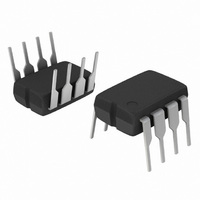
NCP1203P60G ON Semiconductor, NCP1203P60G Datasheet - Page 9

NCP1203P60G
Manufacturer Part Number
NCP1203P60G
Description
IC CTRLR PWM CM UVLO HV 8DIP
Manufacturer
ON Semiconductor
Datasheet
1.NCP1203P100G.pdf
(15 pages)
Specifications of NCP1203P60G
Output Isolation
Isolated
Frequency Range
57 ~ 73kHz
Voltage - Input
8.4 ~ 16 V
Voltage - Output
500V
Operating Temperature
-40°C ~ 150°C
Package / Case
8-DIP (0.300", 7.62mm)
Number Of Outputs
1
Duty Cycle (max)
80 % (Typ)
Output Current
250 mA
Mounting Style
Through Hole
Switching Frequency
65 KHz (Typ)
Operating Supply Voltage
16 V
Maximum Operating Temperature
125 C
Fall Time
28 ns
Minimum Operating Temperature
- 40 C
Rise Time
67 ns
Synchronous Pin
No
Topology
Flyback
Lead Free Status / RoHS Status
Lead free / RoHS Compliant
Other names
NCP1203P60GOS
Available stocks
Company
Part Number
Manufacturer
Quantity
Price
Company:
Part Number:
NCP1203P60G
Manufacturer:
ON Semiconductor
Quantity:
8 500
Part Number:
NCP1203P60G
Manufacturer:
ON/安森美
Quantity:
20 000
Calculating the V
consumption as soon as V
NCP1203P60 is used and drives a MOSFET with a 30 nC
total gate charge (Qg). The total average current is thus made
of ICC1 (700 mA) plus the driver current, Fsw x Qg or
1.8 mA. The total current is therefore 2.5 mA. The ΔV
available to fully startup the circuit (e.g. never reach the
7.8 V UVLO during power on) is 12.8–7.8 = 5 V. We have
a capacitor who then needs to supply the NCP1203 with
2.5 mA during a given time until the auxiliary supply takes
over. Suppose that this time was measured at around 15 ms.
CV
Skipping Cycle Mode
the output power demand drops below a given level. This is
accomplished by monitoring the FB pin. In normal
operation, pin 2 imposes a peak current accordingly to the
load value. If the load demand decreases, the internal loop
asks for less peak current. When this setpoint reaches a
determined level (Vpin 1), the IC prevents the current from
decreasing further down and starts to blank the output
pulses: the IC enters the so- -called skip cycle mode, also
named controlled burst operation. The power transfer now
depends upon the width of the pulse bunches (Figure 17).
Suppose we have the following component values:
Lp, primary inductance = 350 mH
Fsw , switching frequency = 61 kHz
Ip skip = 600 mA (or 333 mV/Rsense)
C ≥ 7.5 mF
The V
The NCP1203 automatically skips switching cycles when
CC
is calculated using the equation
CC
. Select a 22 mF/16 V and this will fit.
capacitor can be calculated knowing the IC
CC
Capacitor
CC
reaches 12.8 V. Suppose that a
Figure 15. Typical Waveforms in Short Circuit Conditions
12.8 V
7.8 V
C =
Δt · i
ΔV
http://onsemi.com
4.9 V
or
9
The theoretical power transfer is therefore:
If this IC enters skip cycle mode with a bunch length of
10 ms over a recurrent period of 100 ms, then the total power
transfer is:
a look at the operation mode versus the FB level
immediately gives the necessary insight:
default), the peak current cannot exceed 1.0 V/Rsense.
When the IC enters the skip cycle mode, the peak current
cannot go below Vpin1/3.3/Rsense. The user still has the
flexibility to alter this 1.0 V by either shunting pin 1 to
ground through a resistor or raising it through a resistor up
to the desired level. Grounding pin 1 permanently
invalidates the skip cycle operation. However, given the
extremely low standby power the controller can reach, the
PWM in no- -load conditions can quickly enter the minimum
t
place. We recommend in that case to leave a little bit of skip
level to always allow 0% duty cycle.
FB
on
DRIVING PULSES
To better understand how this skip cycle mode takes place,
When FB is above the skip cycle threshold (1.0 V by
and still transfer too much power. An instability can take
NORMAL CURRENT
MODE OPERATION
SKIP CYCLE OPERATION
I
P(min)
V
CC
= 333 mV/R
3.8 . 0.1 = 380 mW
1
2
· Lp · Ip 2 · Fsw = 3.8 W
SENSE
Figure 16.
.
4.2 V, FB Pin Open
3.2 V, Upper
Dynamic Range
1 V


