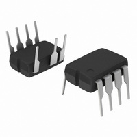
NCP1230P100G ON Semiconductor, NCP1230P100G Datasheet - Page 2

NCP1230P100G
Manufacturer Part Number
NCP1230P100G
Description
IC CTRLR PWM SMPS OVP OCP 7DIP
Manufacturer
ON Semiconductor
Datasheet
1.NCP1230P100G.pdf
(21 pages)
Specifications of NCP1230P100G
Output Isolation
Isolated
Frequency Range
100kHz
Voltage - Input
11.6 ~ 18 V
Power (watts)
702mW
Operating Temperature
-40°C ~ 125°C
Package / Case
8-DIP (0.300", 7.62mm), 7 Leads
Number Of Outputs
1
Duty Cycle (max)
80 % (Typ)
Output Voltage
18 V (Max)
Output Current
800 mA (Max)
Mounting Style
Through Hole
Switching Frequency
107 KHz
Operating Supply Voltage
- 0.3 V to + 18 V
Maximum Operating Temperature
+ 150 C
Fall Time
15 ns
Rise Time
40 ns
Synchronous Pin
No
Topology
Flyback
Lead Free Status / RoHS Status
Lead free / RoHS Compliant
Available stocks
Company
Part Number
Manufacturer
Quantity
Price
Company:
Part Number:
NCP1230P100G
Manufacturer:
ON Semiconductor
Quantity:
1 923
Company:
Part Number:
NCP1230P100G
Manufacturer:
ON Semiconductor
Quantity:
110
Part Number:
NCP1230P100G
Manufacturer:
ON/安森美
Quantity:
20 000
PIN FUNCTION DESCRIPTION
HV
Pin No.
+
CBulk
1
2
3
4
5
6
7
8
MC33262/33260
1
2
3
4
Pin Name
PFC V
CS/OVP
GND
DRV
V
NC
HV
FB
CC
CC
8
7
6
5
This pin provides
the bias voltage to
the PFC controller.
Feedback Signal
Current Sense
IC Ground
Driver Output
V
High−Voltage
CC
Function
Input
−
PFC_V
Figure 1. Typical Application Example
OVP
CC
This pin is a direct connection to the V
standby and during the startup sequence, the switch is open and the PFC V
shut down. As soon as the aux. winding is stabilized, Pin 1 connects to the V
and provides bias to the PFC controller. It goes down in standby and fault conditions.
An optocoupler collector pulls this pin low to regulate. When the current setpoint
reaches 25% of the maximum peak, the controller skips cycles.
This pin incorporates three different functions: the current sense function, an internal
ramp compensation signal and a 3.0 V latch−off level which latches the output off
until V
With a drive capability of +500 mA / −800 mA, the NCP1230 can drive large Qg
MOSFETs.
The controller accepts voltages up to 18 V and features a UVLO turn−off threshold of
7.7 V typical.
This pin connects to the bulk voltage and offers a lossless startup sequence. The
charging current is high enough to support the bias needs of a PWM controller
through Pin 1.
http://onsemi.com
1
2
3
4
CC
Ramp Comp
NCP1230
is recycled.
10 k
2
8
7
6
5
OVP
Pin Description
V
CC
CC
Cap
pin (Pin 6) via a low impedance switch. In
−
−
Rsense
GN
D
+
CC
GND
CC
is
V
pin
out


