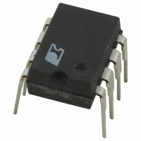
TNY254P Power Integrations, TNY254P Datasheet - Page 6

TNY254P
Manufacturer Part Number
TNY254P
Description
IC OFFLINE SWIT OTP OCP HV 8DIP
Manufacturer
Power Integrations
Series
TinySwitch®r
Datasheet
1.TNY253GN-TL.pdf
(20 pages)
Specifications of TNY254P
Output Isolation
Isolated
Frequency Range
40 ~ 48kHz
Voltage - Output
700V
Power (watts)
4W
Operating Temperature
-40°C ~ 150°C
Package / Case
8-DIP (0.300", 7.62mm)
Output Voltage
5.8 V
Input / Supply Voltage (max)
265 VAC
Input / Supply Voltage (min)
85 VAC
Duty Cycle (max)
68 %
Switching Frequency
44 KHz
Supply Current
140 uA
Operating Temperature Range
- 40 C to + 150 C
Mounting Style
Through Hole
Lead Free Status / RoHS Status
Contains lead / RoHS non-compliant
Available stocks
Company
Part Number
Manufacturer
Quantity
Price
Company:
Part Number:
TNY254P
Manufacturer:
POWER
Quantity:
1 155
Company:
Part Number:
TNY254P
Manufacturer:
POWER
Quantity:
5 510
Part Number:
TNY254P
Manufacturer:
POWER
Quantity:
20 000
Company:
Part Number:
TNY254PN
Manufacturer:
PowerInt
Quantity:
350
Company:
Part Number:
TNY254PN
Manufacturer:
POWER
Quantity:
15 000
Part Number:
TNY254PN
Manufacturer:
POWER
Quantity:
20 000
10 W Standby
The TNY255 is ideal for standby applications that require up to
10 W of power from 230 VAC or 100/115 VAC with doubler
circuit. The TNY255 operates at 130 kHz as opposed to 44 kHz
for TNY253/254. The higher frequency operation allows the
use of a low cost EE16 core transformer up to the 10 W level.
Figure 10 shows a 5 V, 10 W circuit for such an application.
The circuit operates from the high voltage DC supply already
available from the main power supply. Capacitor C1 filters the
high voltage DC supply, and is necessary only if there is a long
trace length from the source of the DC supply to the inputs of the
standby circuit. The high voltage DC bus is applied to the
primary winding of T1 in series with the integrated high voltage
Figure 10. 10 W Standby Supply Circuit.
Figure 9. 1.3 W TV Standby Circuit using TNY253.
TNY253/254/255
6
D
4/03
240-375
VDC
120-375 VDC
DC IN
+
Optional
0.01 F
1 kV
C1
Optional
0.01 µF
1 kV
C1
150 k
1 W
R1
56 pF
1 kV
100 Ω
1/2 W
C2
R1
4700 pF
1 kV
C2
TNY255P
1N4937
TNY253P
D1
U1
U1
D
S
D
S
1
4
1
4
EN
BP
EN
BP
TinySwitch
TinySwitch
T1
T1
MOSFET inside the TNY255. The diode D1, capacitor C2 and
resistor R1 comprise the clamp circuit that limits the turn-off
voltage spike on the TinySwitch DRAIN pin to a safe value.
The secondary winding is rectified and filtered by D2 and C4
to provide the 5 V ouput. Additional filtering is provided by L1
and C5. The output voltage is determined by the sum of the
optocoupler U2 LED forward drop (~ 1 V) and Zener diode
VR1 voltage. The resistor R2, maintains a bias current through
the Zener to improve its voltage tolerance. For tighter tolerance,
a TL431 precision reference IC feedback circuit may be used.
Cellular Phone Charger
The TinySwitch is well suited for applications that require a
0.1 µF
C3
0.1 F
10
8
10
8
C3
1N4934
SB540
D1
Y1 Safety
LTV817
680 pF
D2
U2
C6
2700 F
SFH615-2
6.3 V
1N5235B
C4
VR1
U2
330 µF
1 kΩ
15 µH
R2
10 V
C4
L1
1N5229B
VR1
10 H
68
L1
R2
47 µF
10 V
220 F
C5
10 V
C5
+ 7.5 V
RTN
+ 5 V
RTN
PI-2242-042303
PI-2246-042303


